
Wafer carrying device and method for wafer rewinding

A wafer carrying and wafer technology, applied in the direction of transportation and packaging, conveyor objects, electrical components, etc., can solve the problems of increasing device manufacturing costs, spending huge purchases, prolonging the process, etc., to prevent wafers from slipping, The effect of reducing production costs and shortening the process

Active Publication Date: 2015-11-25
SHANGHAI HUALI MICROELECTRONICS CORP
View PDF7 Cites 0 Cited by
  • Summary
  • Abstract
  • Description
  • Claims
  • Application Information

AI Technical Summary

Problems solved by technology

[0008] In view of the above existing problems, the present invention provides a wafer carrying device and a wafer rewinding method to overcome the need to use rewinding equipment for rewinding in the prior art due to process requirements on the back of the wafer. Prolonging the process, prolonging the process time, and spending a huge amount of money to purchase special rewinding equipment, which leads to the problem of increasing the manufacturing cost of the device, thereby improving production efficiency, eliminating the use of rewinding equipment, and reducing the production cost of the device

Method used


Image

  • Wafer carrying device and method for wafer rewinding
  • Wafer carrying device and method for wafer rewinding
  • Wafer carrying device and method for wafer rewinding

Examples


Embodiment 1

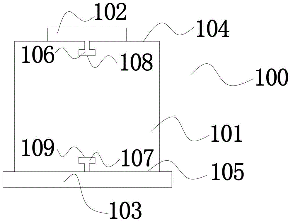
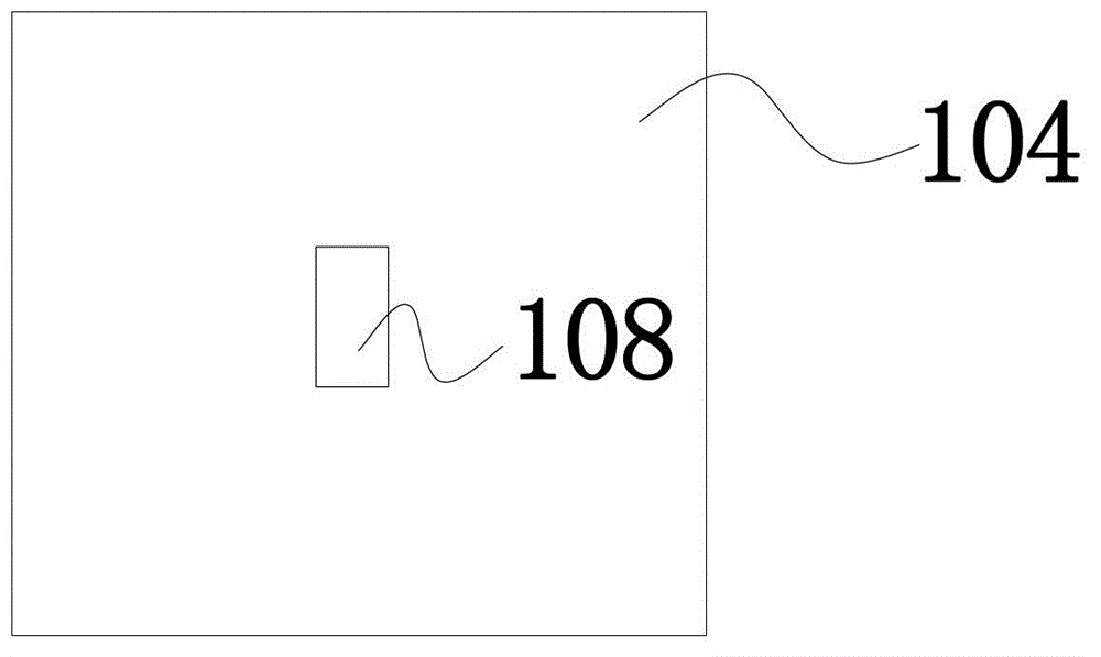
[0043] figure 1It is a schematic diagram of the front structure of the wafer carrying device provided in Embodiment 1 of the present invention; as shown in the figure, the wafer carrying device 100 includes a loading box 101, a trolley lifting module 102 and an identification and positioning module 103, wherein the loading box 101 A card slot 108 is provided on the upper surface 104 of the loading box body 101, and a card slot 109 is provided on the lower surface 105 of the loading box body 101. The card slot 108 and the card slot 109 have the same shape and size; Lifting structure (not shown in the figure), the lower surface of the trolley lifting module 102 is provided with a snap joint 106, and the lower surface of the identification and positioning module 103 is provided with an identification and positioning hole (not shown in the figure), the identification and positioning module 103 The upper surface is provided with a card connector 107, the above-mentioned card connec...

Embodiment 2

[0055] Figure 7 It is a schematic flow chart of the method for wafer rewinding provided by Embodiment 2 of the present invention; as shown in the figure, a detachable trolley lifting module and an identification and positioning module are set on the loading box of a wafer carrying device; reloading The wafer is placed in the loading box; then when the wafer needs to be rewound during the process production, the positions of the trolley lifting module and the identification and positioning module are exchanged, and the loading box is turned over to rewind the wafer ; Finally, the wafer carrying device is transferred to the top of the corresponding process machine by the lifting module of the lifting trolley, and the wafer carrying device is loaded onto the process machine by using the identification and positioning module.

[0056] Wherein, the loading box body also includes a loading box cover plate, and the loading box cover plate is provided with multiple sets of carrying c...


PUM


Abstract

The invention discloses a wafer bearing device and a method for overturning wafers. Due to the facts that a trolley lifting module and a location hole identification module in the wafer bearing device are of a movably detachable structure, a clamping groove formed in the upper surface of a loading box body and a clamping groove formed in the lower surface of the loading box body are the same, and a clamping joint of the trolley lifting module and a clamping joint of the location hole identification module are also the same, the trolley lifting module and the location hole identification module can be conveniently exchanged. In addition, due to the fact that a plurality of sets of elastic bearing clamping grooves which can fix the wafers are formed in a cover plate of a loading box, the wafers can be prevented from sliding when the wafer bearing device is turned over. Therefore, on one hand, the time for overturning the wafers can be saved, the technology process can be effectively shortened, expenditure for purchasing a wafer overturning device is saved, production cost of devices is reduced, and on the other hand, technological waiting time of products can be shortened, and the yield of the products is improved.

Description

technical field [0001] The invention relates to a turnover tool, in particular to a wafer carrying device and a wafer rewinding method. Background technique [0002] Wafer refers to the silicon wafer used in the production of silicon semiconductor integrated circuits. Because of its circular shape, it is called a wafer. It can be processed into various circuit element structures on silicon wafers, which are called IC products with specific electrical functions. Single crystal silicon wafers are drawn and refined from ordinary silica sand, and are made into single crystal silicon rods through a series of measures of dissolution, purification and distillation. After the single crystal silicon rods are polished and sliced, they become wafers. In wafer production, it is often necessary to use turnover tools to transfer materials to the next process, and most manufacturers use carrier boxes for wafer turnover. [0003] The rapid development of integrated circuits has led to inc...

Claims


Application Information

Patent Timeline
Patent Type & Authority Patents(China)
IPC IPC(8): H01L21/673H01L21/677
Inventor 顾海龙裴雷洪严骏
Owner SHANGHAI HUALI MICROELECTRONICS CORP
Learn More