
Surface scanning unit and optical detection device with surface scanning unit

A scanning unit, optical detection technology, applied in electrical components, image communication, etc., can solve the problems of cost-intensive, inability to produce reflection, poor interlacing of light and dark, etc., to achieve the effect of reducing the impact

Active Publication Date: 2016-03-09
YAYATECH
View PDF7 Cites 0 Cited by
  • Summary
  • Abstract
  • Description
  • Claims
  • Application Information

AI Technical Summary

Problems solved by technology

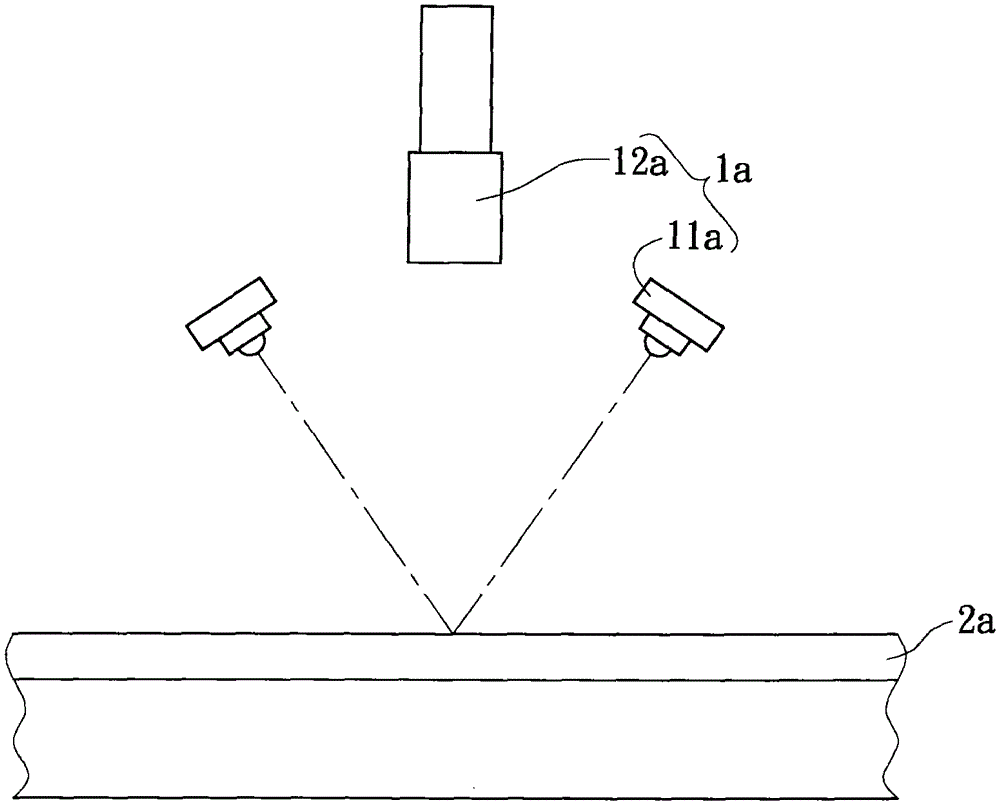
However, if it is necessary to stop the machine to adjust the angle of the linear light source 11a in order to adapt to different situations, it will cost a lot of money virtually
[0005] Furthermore, the focus line is easily affected by the uneven (rough) surface of the printed circuit board 2a to affect the imaging quality
For example: the more vertical the projection angle of the linear light source 11a, the more likely it will be affected by the rough surface of the printed circuit board 2a, thus resulting in poor images with interlaced light and dark
However, the more horizontal the projection angle of the linear light source 11a is, the more difficult it is to reflect light due to the concave portion on the surface of the printed circuit board 2a

Method used


Image

  • Surface scanning unit and optical detection device with surface scanning unit
  • Surface scanning unit and optical detection device with surface scanning unit
  • Surface scanning unit and optical detection device with surface scanning unit

Examples


no. 1 example 〕

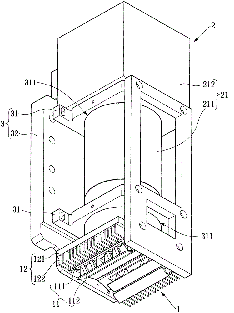
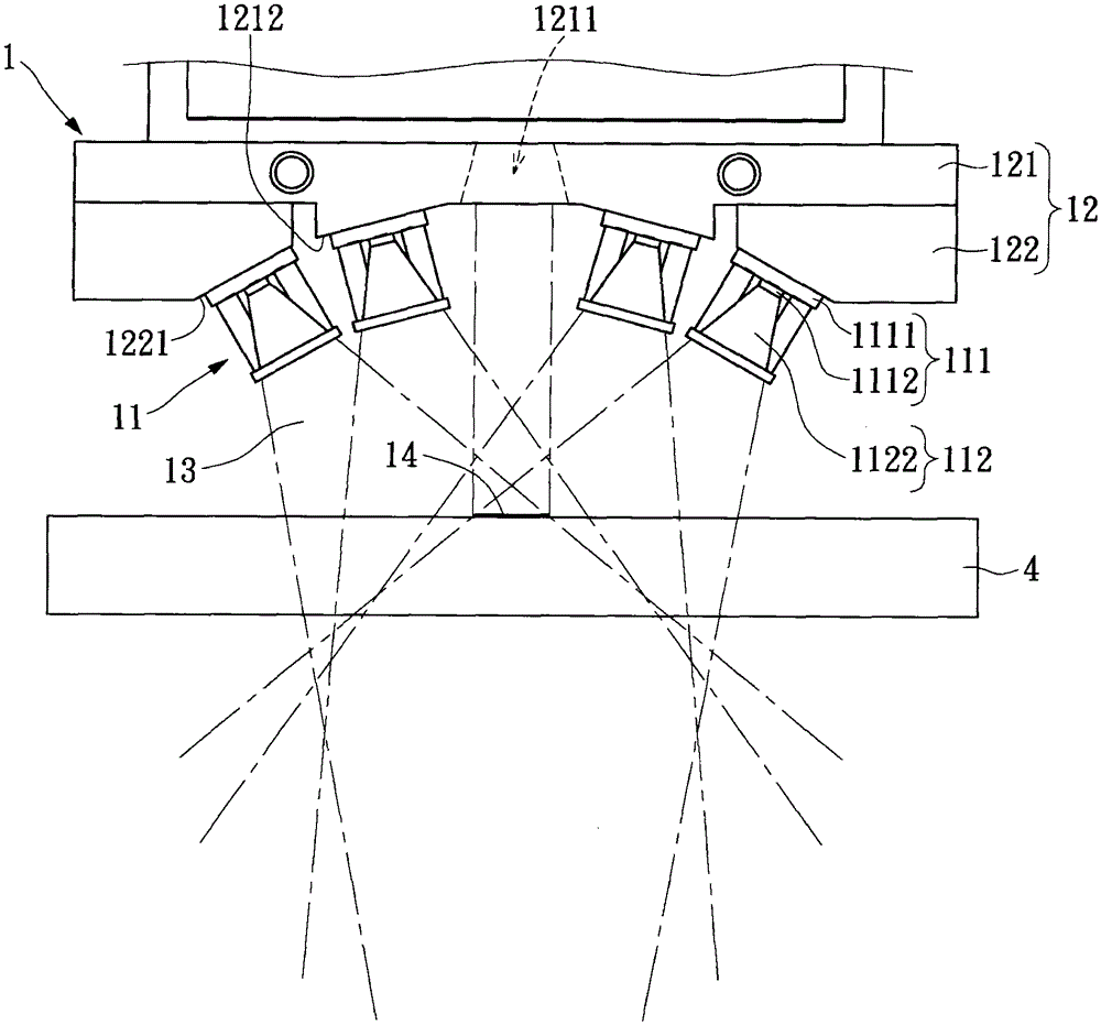
[0061] see Figure 2 to Figure 5 , which is the first embodiment of the present invention, where, figure 2 and Figure 4A to Figure 5 It is a three-dimensional schematic diagram of this embodiment, Figure 3A and Figure 3B It is a schematic plan view of this embodiment.

[0062] Refer again figure 2 and Figure 3A As shown, this embodiment is an optical detection device with a surface scanning unit, which is used for surface scanning and capturing an image of an object under test 4. The object under test 4 is used in this embodiment as a printed circuit board 4 as an example, but not limited thereto. Furthermore, in practical application of this embodiment, the optical detection device can be installed on a slide rail (not shown), and the object to be tested can be installed on a movable platform (not shown).

[0063] The optical detection device includes a surface scanning unit 1 , an imaging unit 2 , and a fixing unit 3 .

[0064] The surface scanning unit 1 inclu...

no. 2 example

[0085] see Figure 6 As shown, it is the second embodiment of the present invention. This embodiment is similar to the first embodiment, and the same parts will not be repeated. The difference between the two mainly lies in the angle positioning module 12 .

[0086] In more detail, the base 121 of the angle positioning module 12 in this embodiment is equivalent to the base 121 described in the first embodiment extending integrally to form the block 122 structure. In other words, the base 121 of this embodiment is formed with two positioning slopes 1212 , 1221 at the same time.


PUM


Abstract

The invention discloses a facial shape scanning unit and an optic detecting device with the facial shape scanning unit. The facial shape scanning unit and the optic detecting device are used for scanning a facial shape and capturing an image of an object to be detected. The optic detecting device comprises the facial shape scanning unit and an image capturing unit. The facial scanning unit comprises a plurality of light source modules which are respectively used for sending a facial shape light ray, the facial shape light rays sent by the plurality of light source modules irradiate the object to be detected respectively from different projecting angles, and the facial shape light rays sent by the plurality of the light source modules form a facial shape scanning block on the surface of the object to be detected in an overlapping mode. The image capturing unit comprises an image pickup module which is used for receiving the light rays reflected by the part, corresponding to the facial scanning block, of the surface of the object to be detected. Therefore, the optic detecting device with the facial shape scanning unit reduces influence of the surface evenness of the object to be detected.

Description

technical field [0001] The invention relates to a scanning unit and an optical detection device, in particular to a surface scanning unit and an optical detection device with the surface scanning unit. Background technique [0002] see figure 1 As shown, it is a schematic diagram of an existing linear scanning detection device. The linear scanning detection device 1a is used for linear scanning and capturing information of a printed circuit board 2a. The linear scanning detection device 1a includes two linear light sources 11a and an imaging module 12a. [0003] Wherein, the positions of the two linear light sources 11a are symmetrical to the printed circuit board 2a and are used to generate linear light, and the light emitted by the two linear light sources 11a forms a focal line on the surface of the printed circuit board 2a. The image capturing module 12a is used for receiving the light reflected by the focal line. [0004] In order to make the light emitted by the two...

Claims


Application Information

Patent Timeline
Patent Type & Authority Patents(China)
IPC IPC(8): H04N1/028H04N1/04
Inventor 陈义谦陈建成吴嘉靖黄宗仁陈礼爵
Owner YAYATECH
Learn More