Embedded type touch screen and display device

An embedded touch screen, touch screen technology, applied in instruments, computing, electrical and digital data processing, etc., can solve the problems of dependence, inability to achieve touch operation, and short life.

Inactive Publication Date: 2013-07-24
HEFEI BOE OPTOELECTRONICS TECH +1
View PDF5 Cites 13 Cited by
  • Summary
  • Abstract
  • Description
  • Claims
  • Application Information

AI Technical Summary

Problems solved by technology

Among them, the resistive sensing type belongs to the low-end sensing technology, and the products produced generally have a short service life; the capacitive sensing type is mainly suitable for small and medium-sized touch screens, that is, touch screens below 10 inches; Restricted, the products produced have a long life and are relatively stable, but the optical sensor touch screen needs to rely on the light environment, and the touch operation cannot be realized without light

Method used


Image

  • Embedded type touch screen and display device
  • Embedded type touch screen and display device
  • Embedded type touch screen and display device

Examples


example 1

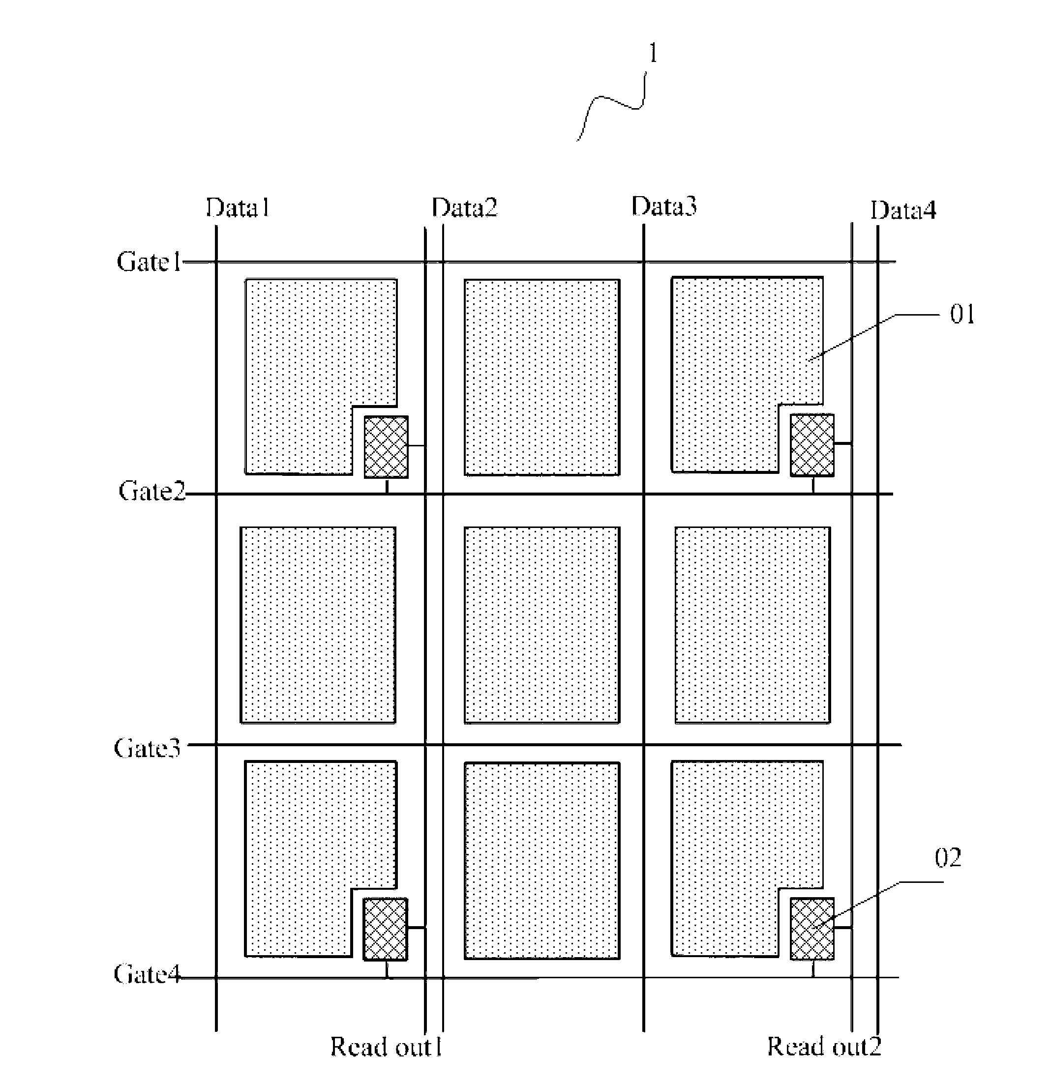
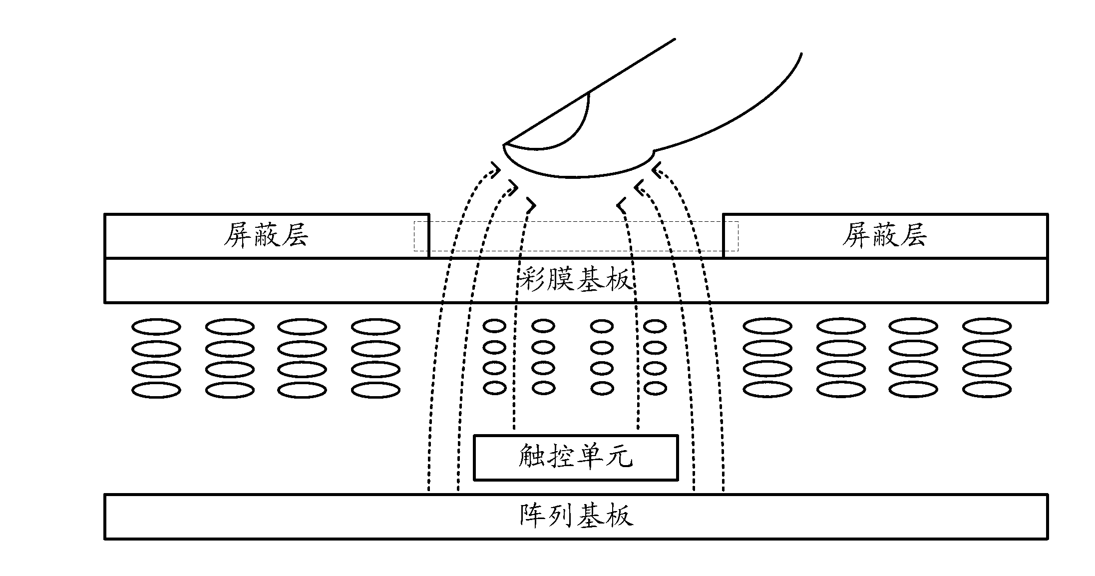
[0035] The array substrate is provided with a plurality of photosensitive scanning lines and a plurality of photosensitive signal lines located between adjacent pixel units in the array substrate. In a specific implementation, the light-sensitive scanning line and the light-sensitive signal line may be arranged at the gap between the pixel units of adjacent rows. Moreover, in order to simplify the wiring on the array substrate, the light-sensitive scan line may be specifically set as at least one gate signal line in the array substrate that is different from the touch scan line. E.g, Figure 3a Gate1 and Gate2 are two adjacent gate signal lines. Gate2 can be used as a touch scan line, Gate1 of the upper row of Gate2 can be used as a photosensitive scan line, and Precharge is a photosensitive signal line. Of course, in specific implementation, the next row of Gate 3 of Gate 2 can also be used as a light-sensitive scanning line, which is not limited here.

[0036] Further, as Fig...

example 2

[0038] A plurality of photosensitive scanning lines located between adjacent pixel units in the array substrate are arranged on the array substrate. In a specific implementation, the light-sensitive scanning line may be arranged at the gap between the pixel units of adjacent rows. Moreover, in order to simplify the wiring on the array substrate, the light-sensitive scan line may be specifically set as at least one gate signal line in the array substrate that is different from the touch scan line. E.g, Figure 3b Gate1 and Gate2 are two adjacent gate signal lines. Gate2 can be used as a touch scan line, and Gate1 in the upper row of Gate2 can be used as a photosensitive scan line. Of course, in specific implementation, the next row of Gate 3 of Gate 2 can also be used as a light-sensitive scanning line, which is not limited here. .

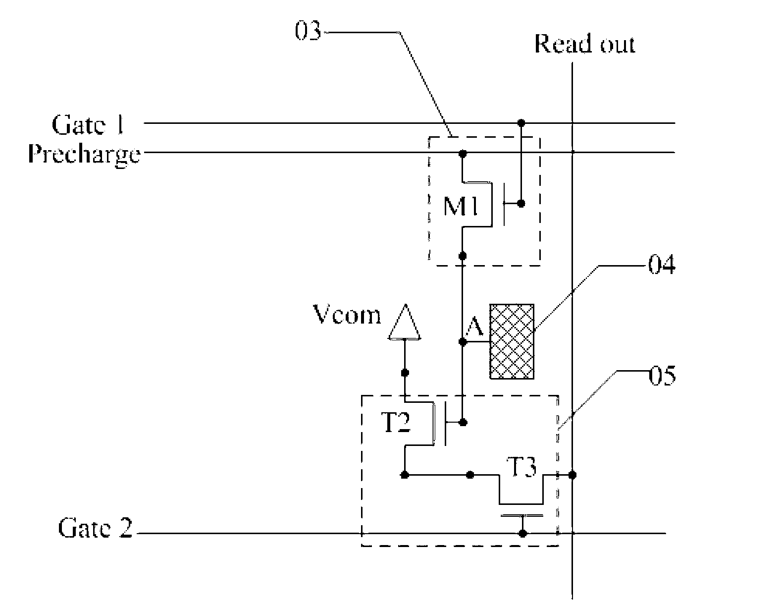
[0039] Such as Figure 3b As shown, the photosensitive subunit 03 includes a photosensitive transistor M1; wherein the gate and source of the photo...

example 3

[0041] A plurality of photosensitive scanning lines located between adjacent pixel units in the array substrate are arranged on the array substrate. In a specific implementation, the light-sensitive scanning line may be arranged at the gap between the pixel units of adjacent rows. Moreover, in order to simplify the wiring on the array substrate, the light-sensitive scan line may be specifically set as at least one gate signal line in the array substrate that is different from the touch scan line. E.g, Figure 3c Gate1 and Gate2 are two adjacent gate signal lines. Gate2 can be used as a touch scan line, and Gate1 of the upper row of Gate2 can be used as a light-sensitive scan line. Of course, in specific implementation, the next row of Gate 3 of Gate 2 can also be used as a light-sensitive scanning line, which is not limited here.

[0042] Such as Figure 3c As shown, the photosensitive subunit 03 includes a photosensitive transistor M1 and a first transistor T1; wherein, the gat...


PUM


Abstract

The invention discloses an embedded type touch screen and a display device. At least one grid electrode signal wire is used as a touch control scanning wire, an array base plate is provided with a touch control reading wire in a position positioned between adjacent array pixel units, and in addition, touch control units are arranged in positions positioned in a region defined by the touch control scanning wire and the touch control reading wire. Each touch control unit consists of a light sensing sub unit, a touch control electrode and a touch control signal control sub unit, the light sensing sub unit is connected with the touch control signal control sub unit through the touch control electrode, and control signals output to the touch control signal control sub unit by the light sensing sub unit change along with the change of the coupling capacitance of the touch control electrode and external light rays. The touch control signal control sub unit is respectively connected with the touch control scanning wire and the touch control reading wire, and when the touch control scanning wire transmits electric signals, the touch control signal control sub unit outputs touch control sensing signals modulated by the control signals via the touch control reading wire. Compared with a single capacitance type touch screen, the embedded type touch screen has the advantage that the touch sensitivity of the touch screen can be improved.

Description

Technical field [0001] The present invention relates to the technical field of liquid crystal display, in particular to an in-cell touch screen and a display device. Background technique [0002] With the rapid development of display technology, touch screen panels have gradually spread throughout people's lives. At present, touch screens can be divided into resistive, capacitive, infrared, surface acoustic wave, electromagnetic, vibration wave induction, and frustrated total internal reflection optical induction according to their working principles. According to the composition structure, the touch screen can be divided into: touch sensing external (double layer), touch sensing on the covering surface (single layer), touch sensing on the panel, and touch sensing inside the panel (embedded). Among them, the structure of the touch sensor inside the panel can not only reduce the overall thickness of the touch screen, but also greatly reduce the manufacturing cost of the touch scr...

Claims


Application Information

Patent Timeline
Patent Type & Authority Applications(China)
IPC IPC(8): G06F3/041
CPCG06F3/0412G06F3/0421G06F3/0443G06F2203/04106G06F2203/04112
Inventor 杨通徐宇博胡明林炳仟
Owner HEFEI BOE OPTOELECTRONICS TECH
Why Eureka
Try Eureka