


Quick Research
Generate reliable direction feasibility study reports for your R&D in just a few steps.

Technical Q&A
Discover and master advanced knowledge NOW. Basics, ideas, possibilities, all at once.

Find Solutions
As an expert in R&D theories, this can generate solutions to your technical problems instantly.

Evaluate Feasibility
Analyze your overall solution with one click, know your potential R&D risks in advance.

Monitor Landscape
Get weekly tech updates, stay abreast of the latest tech innovations and key insights.
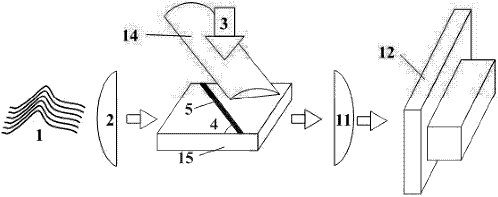
Measuring device of ultrafast optical pulse time wave form
A technology of pulse time and measurement device, applied in the direction of instruments, etc., can solve the problems of affecting the time resolution of measurable signal light, complicated process operation, etc., and achieve the effect of eliminating the space charge effect
- Summary
- Abstract
- Description
- Claims
- Application Information
AI Technical Summary
Problems solved by technology
Method used
Image

Examples
Embodiment Construction
[0022] The device of the present invention will be further described below in conjunction with the embodiments and accompanying drawings, but the protection scope of the present invention should not be limited by this.
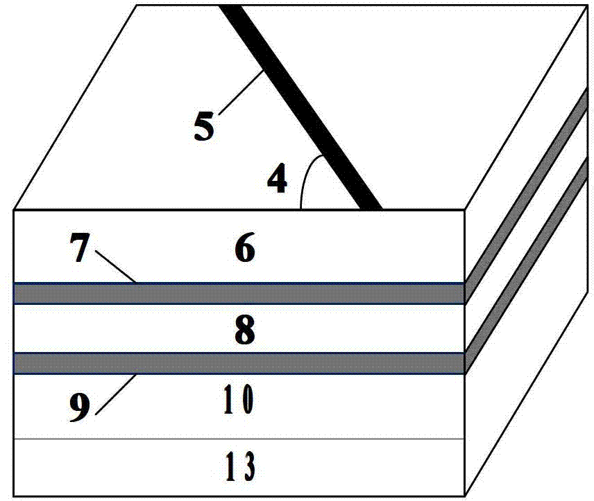
[0023] see first figure 1 , it can be seen from the figure that the measurement device of the ultrafast light pulse time waveform of the present invention. In the optical waveguide, two waveguide cores form a Maserhed (MZ) interferometer, and the two arms of the MZ interferometer are figure 1 7 and 9 here. The initial phase difference of the two arms of the MZ is (2k+1)*π (k is an integer), without the vertically incident pump light 3, when the signal light 1 passes through the MZ interferometer, it reaches an extinction state, and there is no signal at the exit end light exits. When the pump light 3 is added, the pump light 5 focused by the cylindrical lens 14 is vertically incident into the optical waveguide, and at the same time, the entire optical pulse...
PUM
 Abstract
Description
Claims
Application Information
 - R&D Engineer
- R&D Manager
- IP Professional
- Industry Leading Data Capabilities
- Powerful AI technology
- Patent DNA Extraction
Browse by: Latest US Patents, China's latest patents, Technical Efficacy Thesaurus, Application Domain, Technology Topic, Popular Technical Reports.
© 2024 PatSnap. All rights reserved.Legal|Privacy policy|Modern Slavery Act Transparency Statement|Sitemap|About US| Contact US: help@patsnap.com