Package structure of Schottky diode
A Schottky diode and packaging structure technology, applied in electrical components, electrical solid devices, circuits, etc., can solve problems such as affecting the service life of Schottky diodes, affecting product production efficiency and quality, and easy chip rotation. Avoid rotation, reduce footprint, and reduce the effect of volume
- Summary
- Abstract
- Description
- Claims
- Application Information
AI Technical Summary
Problems solved by technology
Method used
Image
Examples
Embodiment Construction
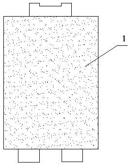
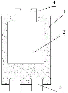
[0019] Such as figure 1 , 2 , 3, and 4, the packaging structure of a Schottky diode of the present invention includes a core
[0020] sheet, jumper 5 and metal frame, the metal frame includes a base metal frame 2 and two lead metal frames 3 opposite to each other at intervals, the lower surface of the chip 6 is welded to the upper surface of the base metal frame 2, and the upper surface of the chip 6 is welded to the jumper One end of the wire 5 and the other end of the jumper 5 are welded on the upper surface of the lead-out metal frame 3, and the base metal frame 2, between and above the lead-out metal frame 3, as well as the top and periphery of the chip 6 and the jumper 5 are covered with a plastic seal. The lower surfaces of the body 1 , the base metal frame 2 and the lead-out metal frame 3 are exposed outside the plastic package 1 , and both the base metal frame 2 and the lead-out metal frame 3 have pins 4 extending outside the plastic package 1 . Since the lower surfa...
PUM
 Abstract
Description
Claims
Application Information
 - R&D
- Intellectual Property
- Life Sciences
- Materials
- Tech Scout
- Unparalleled Data Quality
- Higher Quality Content
- 60% Fewer Hallucinations
Browse by: Latest US Patents, China's latest patents, Technical Efficacy Thesaurus, Application Domain, Technology Topic, Popular Technical Reports.
© 2025 PatSnap. All rights reserved.Legal|Privacy policy|Modern Slavery Act Transparency Statement|Sitemap|About US| Contact US: help@patsnap.com


