Independent double-grid FinFET channel potential distribution analysis model

A technology of potential distribution and channels, which is applied in the direction of electrical digital data processing, special data processing applications, instruments, etc., can solve the problems of reduced effectiveness

Inactive Publication Date: 2013-07-03
SHANGHAI HUALI MICROELECTRONICS CORP
View PDF2 Cites 7 Cited by
  • Summary
  • Abstract
  • Description
  • Claims
  • Application Information

AI Technical Summary

Problems solved by technology

[0004] The purpose of the present invention is to establish a channel potential analytical model by using the series method to solve the two-dimensional Poisson equation for an independent double-gate FinFET, so as to solve a series of assumptions used in solving the two-dimensional Poisson equation in the prior art or approximate conditions that make it less effective when the channel is very short

Method used


Image

  • Independent double-grid FinFET channel potential distribution analysis model
  • Independent double-grid FinFET channel potential distribution analysis model
  • Independent double-grid FinFET channel potential distribution analysis model

Examples


Embodiment Construction

[0028] In order to make the technical means, creative features, goals and effects achieved by the present invention easy to understand, the present invention will be further elaborated below in conjunction with specific illustrations.

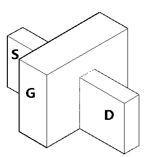
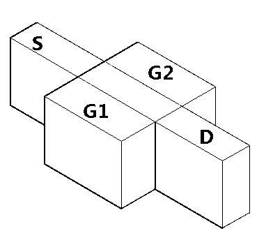
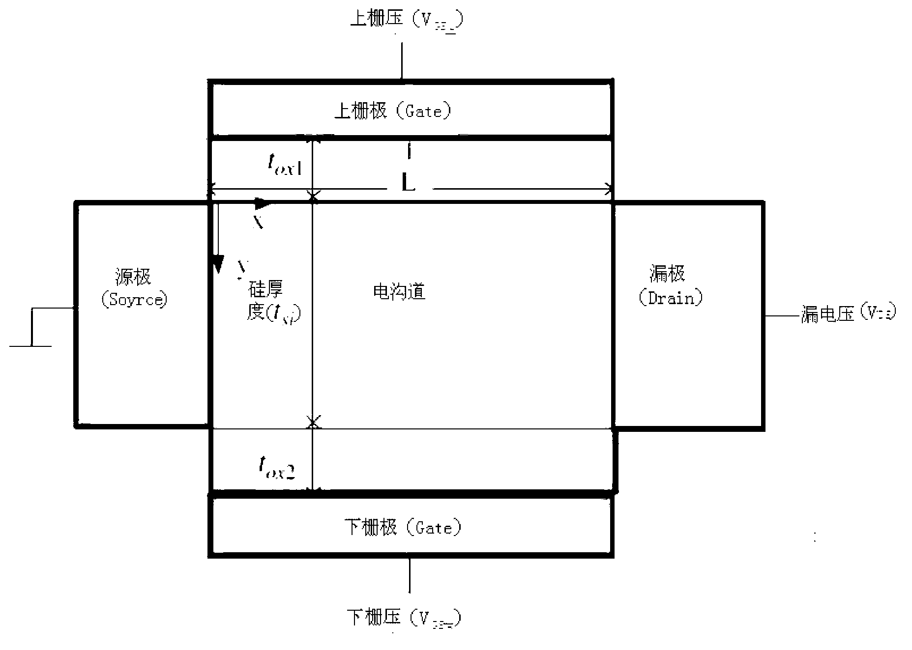
[0029] Such as figure 2 , 3 , 4A and 4B, an independent dual-gate FinFET analytical channel potential distribution model, including: a source on one side of the current-carrying channel, a drain on the side of the current-carrying channel away from the source, and a drain on the side of the current-carrying channel The top surface of the channel is provided with an upper gate, and the bottom surface of the current-carrying channel is provided with a lower gate. The analytical formula of the potential distribution model of the device structure is:

[0030] ψ ( x , y ) = V SS + V ...


PUM


Abstract

The invention provides an independent double-grid FinFET (Fin Field-Effect Transistor) channel potential distribution analysis model which comprises a source electrode, wherein the source electrode is arranged on one side of a powered channel; the side of the powered channel, which is deviated from the powered channel, is provided with a drain electrode; the top surface of the powered channel is provided with an upper grid electrode; and the bottom surface of the powered channel is provided with a lower grid electrode. The independent double-grid FinFET channel potential distribution analysis model is characterized in that the device structure adopts the following potential distribution model analysis formula. The independent double-grid FinFET channel potential distribution analysis model disclosed by the invention does not use more approximate conditions and solves a two-dimensional poisson equation by using a progression method so as to establish a channel potential analysis model; the analysis model adopts more reasonable boundary condition; complex geometrical structure parameters and experimental parameters are not introduced into the analysis model; and the analysis model is suitable for different conditions such as substrate reversed bias voltages, drain voltages and the like, well accords with a numerical simulation result and has the advantages of simple form, high computing accuracy and high computing speed.

Description

technical field [0001] The invention belongs to the technical field of semiconductors, and in particular relates to an independent double-gate FinFET (FinField-Effect Transistor) analytical channel potential distribution model. Background technique [0002] In order to improve the integration level of integrated circuits and the performance of chips, with the development of integrated circuit MOS device technology, the critical dimensions of devices are getting smaller and smaller. For the mainstream single-gate planar process, the gate length of the device cannot be reduced indefinitely, and a series of secondary effects that appear as the device size shrinks are collectively referred to as short-channel effects. The electrical characteristics of the device tend to become poor in the case of short channels. In order to overcome the influence of the short channel effect on the performance and reliability of small-sized MOS devices, some new device structures have emerged, s...

Claims


Application Information

Patent Timeline
Patent Type & Authority Applications(China)
IPC IPC(8): G06F17/50
Inventor 顾经纶颜丙勇
Owner SHANGHAI HUALI MICROELECTRONICS CORP
Why Eureka
Try Eureka