Nor FLASH memory interface module applied to configurable logic block (CLB) bus
A storage interface and bus technology, which is applied in the field of built-in NorFLASH storage interface modules, can solve the problems of cumbersome operation steps, multiple CPU resources, and many signals, and achieve the effect of simple read and write operation steps, strong versatility, and improved utilization
- Summary
- Abstract
- Description
- Claims
- Application Information
AI Technical Summary
Problems solved by technology
Method used
Image
Examples
Embodiment
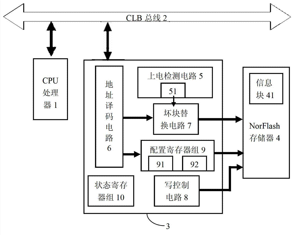
[0028] Embodiment: a NorFLASH storage interface module applied to the CLB bus, a NorFlash memory 4 communicates with the CPU processor 1 via the CLB bus 2 through the NorFLASH storage interface module 3, and the NorFLASH storage interface module 3 further includes power-on detection Circuit 5, address decoding circuit 6, bad block replacement circuit 7, write control circuit 8, configuration register group 9 and status register group 10 for displaying the last operating state;
[0029] There is an information block 41 in the described NorFlash memory 4, and this information block 41 records the address of the bad block unit in the NorFlash memory 4, the address of the number, the replacement unit and the replacement unit to replace the bad block function enabling bit information, and this enabling bit is effective There is a bad block in the identification NorFlash memory 4, and there is a bad block register 51 for storing bad block information from the information block 41 in ...
PUM
 Abstract
Description
Claims
Application Information
 - R&D
- Intellectual Property
- Life Sciences
- Materials
- Tech Scout
- Unparalleled Data Quality
- Higher Quality Content
- 60% Fewer Hallucinations
Browse by: Latest US Patents, China's latest patents, Technical Efficacy Thesaurus, Application Domain, Technology Topic, Popular Technical Reports.
© 2025 PatSnap. All rights reserved.Legal|Privacy policy|Modern Slavery Act Transparency Statement|Sitemap|About US| Contact US: help@patsnap.com


