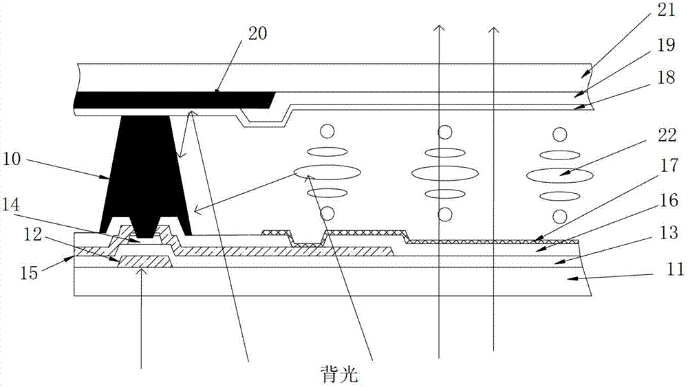
A liquid crystal display device
A technology of liquid crystal display devices and thin film transistors, which is applied in the direction of optics, optomechanical equipment, instruments, etc., can solve problems such as the stability of liquid crystal display devices, and achieve the effect of avoiding light-induced leakage current and weakening light-generated leakage current
- Summary
- Abstract
- Description
- Claims
- Application Information
AI Technical Summary
Problems solved by technology
Method used
Image
Examples
Embodiment 1
[0042] This embodiment discloses a liquid crystal display device, such as figure 1 shown, including:
[0043] The array substrate and the color filter substrate arranged oppositely, and the opaque spacer 10 between the array substrate and the color filter substrate.
[0044] Wherein, the array substrate includes:
[0045] The first transparent substrate 11 is preferably a glass substrate.
[0046] The gate lines 12 are located on the surface of the transparent substrate 11 . Wherein, the gate line 12 is specifically divided into a gate scan line and a gate.
[0047] The first protective layer 13 covers the gate lines 12 and the surface of the first transparent substrate 11 , and the first protective layer 13 is transparent.
[0048] A silicon island 14 , the silicon island 14 is made of amorphous silicon, is located on the surface of the first protection layer 13 , and the silicon island 14 is located directly above the gate of the gate line 12 . It can be seen that the l...
Embodiment 2
[0061] This embodiment discloses a method for manufacturing a liquid crystal display device, the method comprising:
[0062] Step S11, such as figure 2 As shown, an array substrate 101 is provided, and the array substrate 101 includes a first transparent substrate, gate lines, a first protection layer, silicon islands, data lines, a second protection layer and pixel electrodes.
[0063] Step S12 , forming a spacer above the thin film transistor of the array substrate, the spacer being an opaque spacer.
[0064] Specifically, the process of forming a spacer includes:
[0065] Such as image 3 As shown, an opaque photosensitive material is coated on the surface of the array substrate 101 to form an opaque layer 102. The opaque photosensitive material preferably includes 12% to 25% of photosensitive acrylic resin and 10% to 25% of photosensitive acrylic monomer. 25%, photosensitizer 2%~10%, stabilizer 0.3%~2%, propylene glycol monomethyl ether ester 50%~70% and carbon black 3...
Embodiment 3
[0072] This embodiment discloses another method for manufacturing a liquid crystal display device, the method comprising:
[0073] Step S21 , providing a color filter substrate, which includes a second transparent substrate, a black matrix, an ink layer, and a common electrode.
[0074] Step S22 , forming spacers on the surface of the color filter substrate, the spacers being opaque spacers.
[0075] Specifically, the process of forming a spacer includes:
[0076] An opaque photosensitive material is coated on the surface of the color filter substrate to form an opaque layer. The opaque photosensitive material preferably includes 12% to 25% of photosensitive acrylic resin, 10% to 25% of photosensitive acrylic monomer, and photosensitive 2%~10% agent, 0.3%~2% stabilizer, 50%~70% propylene glycol monomethyl ether ester and 3%~8% carbon black.
[0077] The opaque layer is exposed to light by using the mask with the sub-pattern of the gap as a mask, and the sub-pattern of the ga...
PUM
 Abstract
Description
Claims
Application Information
 - R&D Engineer
- R&D Manager
- IP Professional
- Industry Leading Data Capabilities
- Powerful AI technology
- Patent DNA Extraction
Browse by: Latest US Patents, China's latest patents, Technical Efficacy Thesaurus, Application Domain, Technology Topic, Popular Technical Reports.
© 2024 PatSnap. All rights reserved.Legal|Privacy policy|Modern Slavery Act Transparency Statement|Sitemap|About US| Contact US: help@patsnap.com


