Array substrate and manufacturing method thereof as well as display device

A technology of an array substrate and a manufacturing method, applied in the display field, can solve the problems affecting the normal charge and discharge of pixels, the large load of the display panel, the pull-up of the common electrode signal, etc., and achieve the effect of reducing the greening phenomenon of the picture and improving the picture quality.

Active Publication Date: 2015-06-17
BOE TECH GRP CO LTD +1
View PDF3 Cites 0 Cited by
  • Summary
  • Abstract
  • Description
  • Claims
  • Application Information

AI Technical Summary

Problems solved by technology

[0003] For large-size full HD ADS (Advanced Super Dimension Switch, advanced super-dimensional field switching technology) panels, due to the high resolution and the large C of ADS pixels st (the storage capacitor between the pixel electrode and the common electrode), which makes the load of the display panel relatively large, and the coupling between the data signal and the common electrode signal also increases, causing the common electrode signal to be pulled up by the data signal, such as figure 1 V shown com Level Shift phenomenon, V com Signal distortion will affect the normal charging and discharging of pixels, which will eventually cause the phenomenon of greenish on the screen, especially the greenish phenomenon in the lower left corner of the display panel

Method used


Image

  • Array substrate and manufacturing method thereof as well as display device
  • Array substrate and manufacturing method thereof as well as display device
  • Array substrate and manufacturing method thereof as well as display device

Examples


Embodiment Construction

[0025] In order to make the technical problems, technical solutions and advantages to be solved by the embodiments of the present invention clearer, the following will describe in detail with reference to the drawings and specific embodiments.

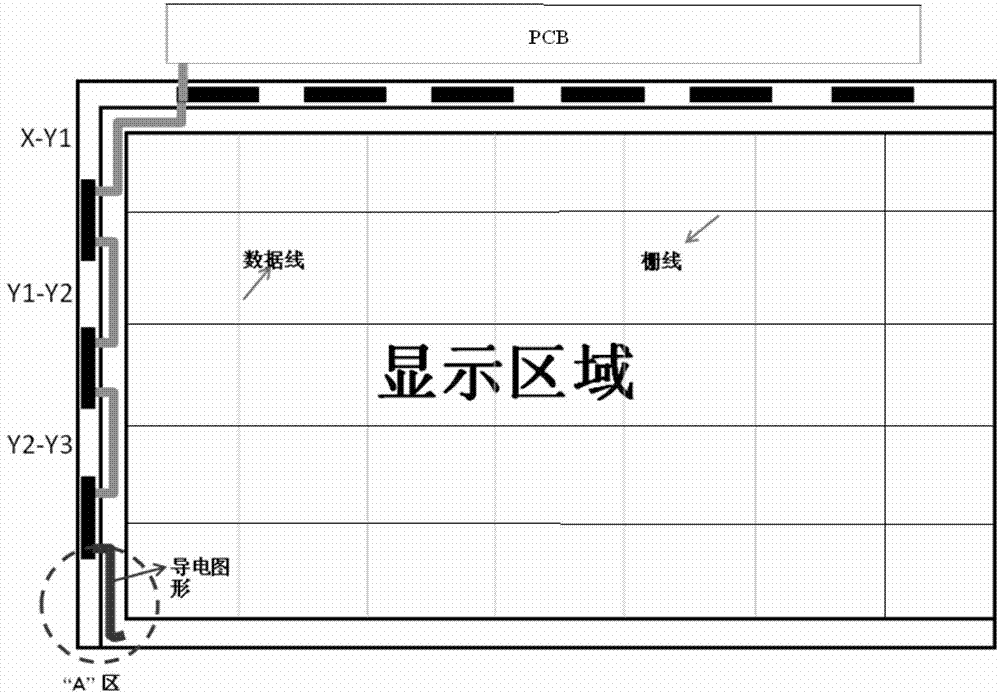
[0026] The embodiment of the present invention aims at the common electrode signal being pulled up by the data signal in the prior art, and V com Level Shift phenomenon, V com Signal distortion affects the normal charging and discharging of pixels, which eventually causes the problem of greening of the picture. An array substrate and its manufacturing method and display device are provided, which can effectively improve the phenomenon of greening of the picture of the display panel and improve the quality of the picture.

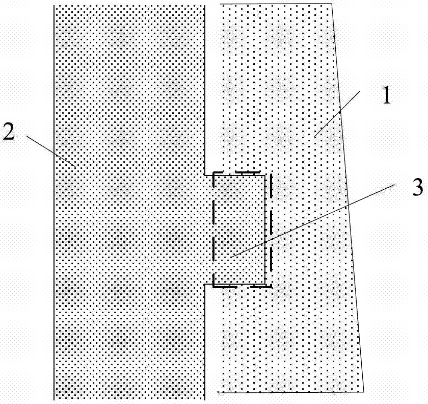
[0027] The array substrate of the present invention includes a substrate and a common electrode pattern and an insulating layer on the substrate, wherein a conductive pattern connected to a low-level potential is for...


PUM


Abstract

The invention provides an array substrate and a manufacturing method of the array substrate as well as a display device, belonging to the field of display technologies. The array substrate comprises a substrate, and a pattern of a public electrode and an insulating layer which are arranged on the substrate, wherein the conductive pattern connected with low-level electric potential is formed on the substrate; and the conductive pattern, the insulating layer and the pattern of the public electrode have an overlapping area, so that a filter capacitor can be formed. The technical scheme of the invention is capable of effectively improving the phenomenon that the picture of a display panel gets green, thus improving the picture quality.

Description

technical field [0001] The present invention relates to the field of display technology, in particular to an array substrate, a manufacturing method thereof, and a display device. Background technique [0002] With the continuous advancement of flat panel display technology, liquid crystal displays have been widely used in display devices such as notebooks, detectors, and TVs. [0003] For large-size full HD ADS (Advanced Super Dimension Switch, advanced super-dimensional field switching technology) panels, due to the high resolution and the large C of ADS pixels st (the storage capacitor between the pixel electrode and the common electrode), which makes the load of the display panel relatively large, and the coupling between the data signal and the common electrode signal also increases, causing the common electrode signal to be pulled up by the data signal, such as figure 1 V shown com Level Shift phenomenon, V com Signal distortion will affect the normal charging and ...

Claims


Application Information

Patent Timeline
Patent Type & Authority Patents(China)
IPC IPC(8): G02F1/1362H01L27/12H01L21/77
Inventor 王骁
Owner BOE TECH GRP CO LTD
Why Eureka
Try Eureka