Method for manufacturing organic electroluminescent display panel, and device for manufacturing organic electroluminescent display panel
A technology of a display panel and a manufacturing method, which is applied in the directions of identification devices, lighting devices, semiconductor/solid-state device manufacturing, etc., can solve the problems of complex control of inkjet devices and the like
- Summary
- Abstract
- Description
- Claims
- Application Information
AI Technical Summary
Problems solved by technology
Method used
Image
Examples
Embodiment approach 1
[0049] [the whole frame]
[0050] figure 1 It is a partial cross-sectional view showing the structure of the organic EL display panel 100 according to the first embodiment. The organic EL display panel 100 is a so-called top emission type in which the upper side in the figure is defined as a display surface.
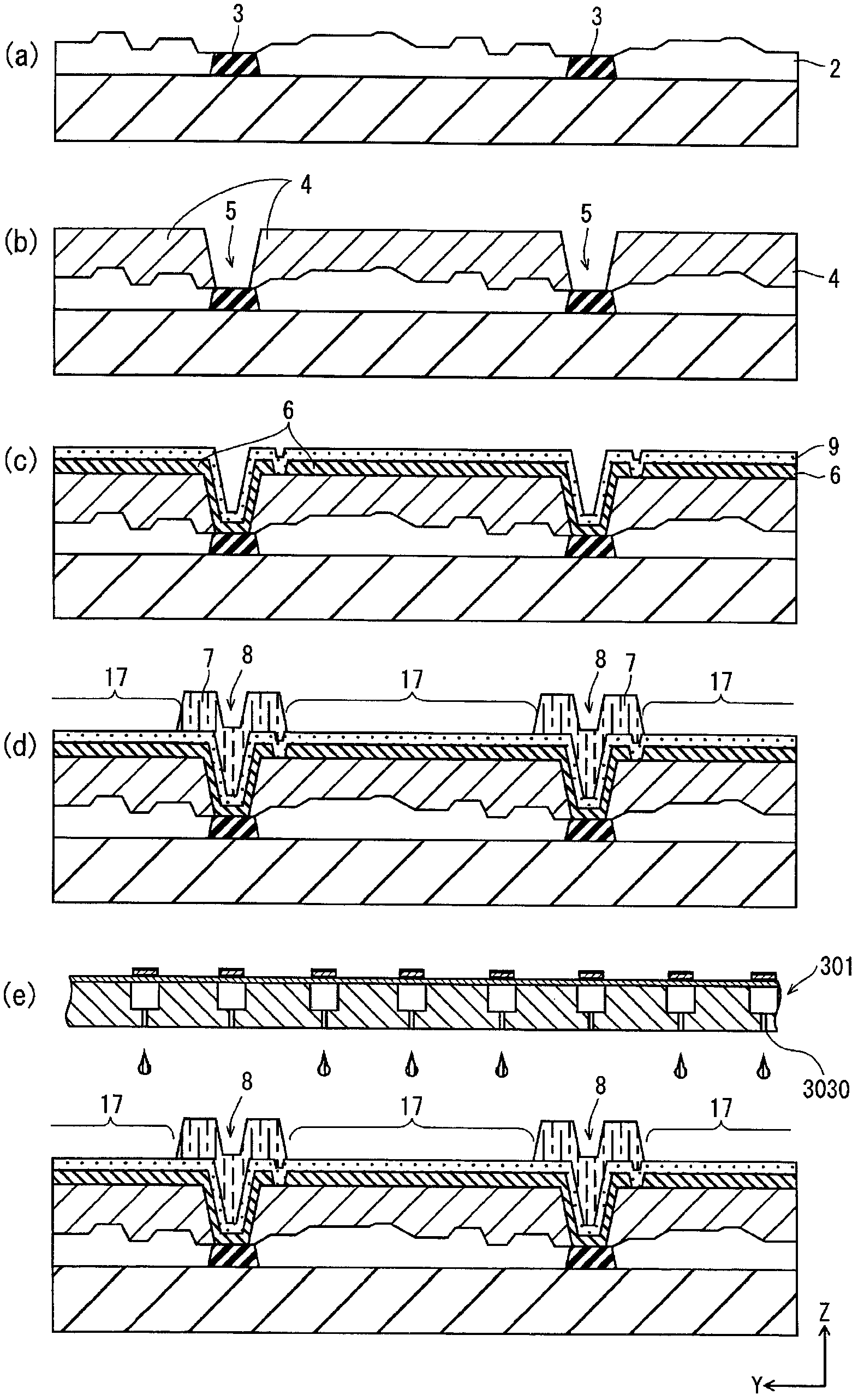
[0051] like figure 1 As shown, a TFT layer 2 , a power supply electrode 3 , a planarization film 4 , a pixel electrode 6 , and a hole injection layer 9 are sequentially stacked on a substrate (EL substrate) 1 . On the hole injection layer 9 , the partition wall layer 7 is provided with a plurality of openings 17 serving as formation regions of the organic light emitting layer 11 . Inside the opening 17 , the hole transport layer 10 , the organic light-emitting layer 11 , the electron transport layer 12 , the electron injection layer 13 , and the counter electrode 14 are laminated in this order.
[0052]
[0053] The substrate 1 is a rear substrate of the organic EL...
Embodiment approach 2
[0219] Figure 18 It is a diagram showing the control flow of the ejection frequency control unit in the step of selecting nozzles for ejecting liquid droplets according to the second embodiment.
[0220] Figure 18 Steps S901, S902, S904-S906, S908-S911 in the Figure 9 S201, S202, S204~S206, S208~S211 in the corresponding. and Figure 9 The difference is that S912A and S913A are provided.
[0221] In this embodiment, when the judgment is N A When ×T is less than the necessary number of discharges N (droplets equal to or greater than the target value cannot be discharged only by the A-class nozzle) (No in step S902), it is determined whether the maximum number of discharges T can be further increased (step S912A). The maximum number of discharges T can be increased by changing the waveform of the drive voltage applied to the piezoelectric element to increase the discharge frequency, or by reducing the scanning speed of the inkjet head.
[0222] When it is determined tha...
PUM
| Property | Measurement | Unit |
|---|---|---|
| Thickness | aaaaa | aaaaa |
Abstract
Description
Claims
Application Information
 - Generate Ideas
- Intellectual Property
- Life Sciences
- Materials
- Tech Scout
- Unparalleled Data Quality
- Higher Quality Content
- 60% Fewer Hallucinations
Browse by: Latest US Patents, China's latest patents, Technical Efficacy Thesaurus, Application Domain, Technology Topic, Popular Technical Reports.
© 2025 PatSnap. All rights reserved.Legal|Privacy policy|Modern Slavery Act Transparency Statement|Sitemap|About US| Contact US: help@patsnap.com


