Light source device
A technology of a light source device and a light guide plate, which is applied in the field of optical components, can solve the problems of local color shift of the light guide plate, the problem of chromatic aberration that cannot be adjusted, and the color difference of the display screen, so as to achieve the effect of reducing the phenomenon of bright spots and the problem of local color shift
- Summary
- Abstract
- Description
- Claims
- Application Information
AI Technical Summary
Problems solved by technology
Method used
Image
Examples
no. 1 example
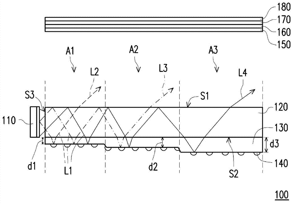
[0038] figure 1 It is a schematic diagram of the light source device according to the first embodiment of the present invention. Please refer to figure 1 , the light source device 100 of this embodiment includes a light emitting element 110 , a light guide plate 120 , an optical film 130 and a plurality of microstructures 140 . The light emitting element 110 is used for providing an illumination light beam L1. In this embodiment, the light emitting element 110 is, for example, a light emitting diode (LED), and the illumination light beam L1 is, for example, white light, wherein the white light is composed of a plurality of color light beams of different colors.
[0039] Such as figure 1 As shown, the light-emitting element 110 is disposed beside the light guide plate 120, and the light guide plate 120 is divided into a plurality of light-transmitting regions A1-A3 (only three are schematically shown). Besides, the light guide plate 120 has a surface S1 , a surface S2 and a...
no. 2 example
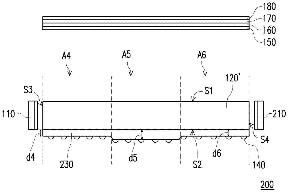
[0050] image 3 It is a schematic diagram of a light source device according to the second embodiment of the present invention. Such as image 3 As shown, the light source device 200 and figure 1 The light source device 100 is similar, but the main difference between the two is that: the light source device 200 further includes a light emitting element 210, and the light guide plate 120' also has a light incident surface S4 opposite to the light incident surface S3. Wherein the light emitting element 210 is disposed beside the light incident surface S4. In this embodiment, the light emitting element 210 is, for example, a white light emitting diode.
[0051] In addition, the thickness of the optical film 230 near the light-emitting element 110 and the light-emitting element 210 is smaller than the thickness of the optical film 230 at the place away from the light-emitting element 110 and the light-emitting element 210 . In other words, compared to the optical film 230 in t...
PUM
 Abstract
Description
Claims
Application Information
 - Generate Ideas
- Intellectual Property
- Life Sciences
- Materials
- Tech Scout
- Unparalleled Data Quality
- Higher Quality Content
- 60% Fewer Hallucinations
Browse by: Latest US Patents, China's latest patents, Technical Efficacy Thesaurus, Application Domain, Technology Topic, Popular Technical Reports.
© 2025 PatSnap. All rights reserved.Legal|Privacy policy|Modern Slavery Act Transparency Statement|Sitemap|About US| Contact US: help@patsnap.com


