A method of manufacturing an array substrate
A manufacturing method and array substrate technology, applied in semiconductor/solid-state device manufacturing, electrical components, circuits, etc., can solve the problems of fast etching rate and over-engraving, and achieve the effect of ensuring uniformity
- Summary
- Abstract
- Description
- Claims
- Application Information
AI Technical Summary
Problems solved by technology
Method used
Image
Examples
Embodiment 1
[0051] The manufacturing method of the array substrate of the present invention comprises the following steps:
[0052] Step S101, forming an IGZO oxide material on a substrate to be patterned with an IGZO oxide semiconductor active layer;
[0053] Step S102, forming a photoresist on the substrate after the previous step;
[0054] Step S103, exposing and developing the substrate in the previous step;
[0055] Step S201, soaking the exposed and developed substrate to be patterned with an IGZO oxide semiconductor active layer with water;
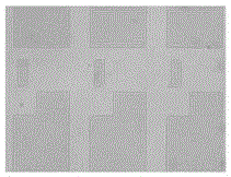
[0056]In step S202, acid gas etching is performed on the wetted substrate, the temperature of the acid gas etching solution (DIEA09) is 40° C., and the etching time is 20 s.
[0057] Step S301, take out the substrate, peel off the photoresist, and obtain such as Figure 4 The array substrate shown.
Embodiment 2
[0059] The manufacturing method of the array substrate of the present invention comprises the following steps:
[0060] Step S101, forming an IGZO oxide material on a substrate to be patterned with an IGZO oxide semiconductor active layer;
[0061] Step S102, forming a photoresist on the substrate after the previous step;
[0062] Step S103, exposing and developing the substrate in the previous step;
[0063] Step S201, soaking the exposed and developed substrate to be patterned with an IGZO oxide semiconductor active layer with water;
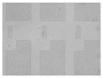
[0064] In step S202, acid gas etching is performed on the wetted substrate, the temperature of the acid gas etching solution (DIEA09) is 50° C., and the etching time is 20 s.
[0065] Step S301, take out the substrate, peel off the photoresist, and obtain such as Figure 5 The array substrate shown.
Embodiment 3
[0067] The manufacturing method of the array substrate of the present invention comprises the following steps:
[0068] Step S101, forming an IGZO oxide material on a substrate to be patterned with an IGZO oxide semiconductor active layer;
[0069] Step S102, forming a photoresist on the substrate after the previous step;
[0070] Step S103, exposing and developing the substrate in the previous step;
[0071] Step S201, soaking the exposed and developed substrate to be patterned with an IGZO oxide semiconductor active layer with water;
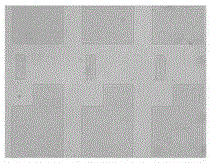
[0072] In step S202, acid gas etching is performed on the wetted substrate, the temperature of the acid gas etching solution (DIEA09) is 45° C., and the etching time is 20 s.
[0073] Step S301, take out the substrate, peel off the photoresist, and obtain such as Figure 6 The array substrate shown.
PUM
 Abstract
Description
Claims
Application Information
 - R&D
- Intellectual Property
- Life Sciences
- Materials
- Tech Scout
- Unparalleled Data Quality
- Higher Quality Content
- 60% Fewer Hallucinations
Browse by: Latest US Patents, China's latest patents, Technical Efficacy Thesaurus, Application Domain, Technology Topic, Popular Technical Reports.
© 2025 PatSnap. All rights reserved.Legal|Privacy policy|Modern Slavery Act Transparency Statement|Sitemap|About US| Contact US: help@patsnap.com


