Aging carrier for electronic products and aging testing method
A technology for aging testing of electronic products, applied in the direction of measuring electricity, measuring devices, measuring electrical variables, etc., can solve problems such as inability to guarantee connection reliability and stability, many internal components of the carrier, and loose internal components, etc., to achieve aging The effect of detection, eliminating lead wires and eliminating solder joints
- Summary
- Abstract
- Description
- Claims
- Application Information
AI Technical Summary
Problems solved by technology
Method used
Image
Examples
Embodiment 1
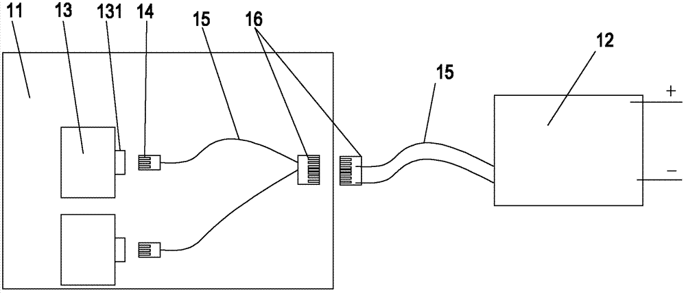
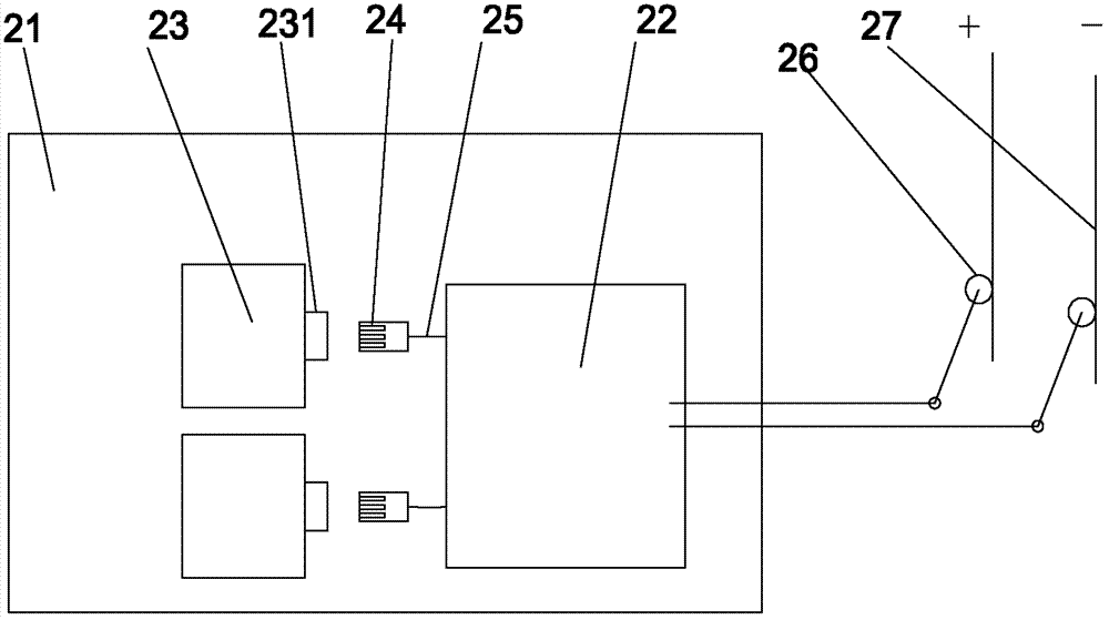
[0048] An electronic product burn-in device in an embodiment of the present application includes a carrier, a circuit board interface, a burn-in cabinet, and a burn-in test system (CPU). The electronic product refers to a power charger or other electronic products that require aging tests.
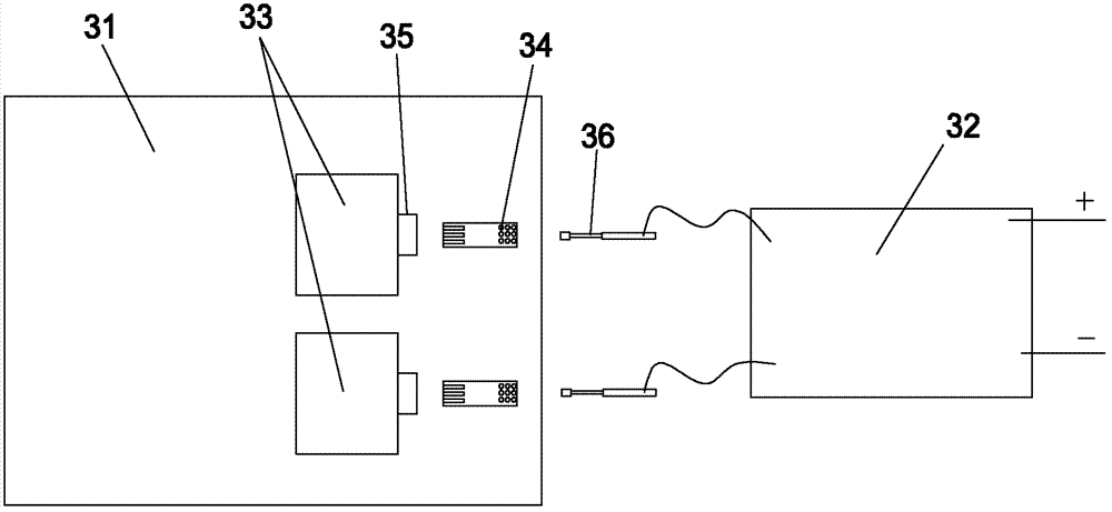
[0049] It is different from the existing technology in which the product to be tested is connected to the cable trough through the lead wire, and then connected to the CPU through the cable trough, please refer to Figure 7 with Figure 8In this example, the circuit board transfer interface 34 used to connect the product under test to the CPU includes a circuit board (PCB) and a soft rubber sleeve 343 . This circuit board is integrated with the input terminal 341 that is used to be connected with electronic product and the output terminal 342 that is used to be connected with burn-in test system (as being used for the CPU of burn-in test), because output terminal 342 and input terminal 34...
Embodiment 2
[0060] The difference between this embodiment and the first embodiment is that the carrier further includes the circuit board transfer interface described in the first embodiment.
Embodiment 3
[0062] The present application also provides an embodiment of an aging test method for electronic products, which includes steps:
[0063] A1. Place the electronic product to be tested in the product placement position of the carrier.
[0064] The carrier in this step can be any carrier described in Embodiment 1.
[0065] A2. Install the circuit board transfer interface with contacts or probes as output terminals on the transfer interface installation position of the carrier.
[0066] The carrier referred to in this step is the carrier mentioned in step A1, and the circuit board adapter refers to the adapter that integrates the input terminal and the output terminal on the same circuit board, which can save the lead wire and solder joint , to eliminate concerns about not being able to guarantee connection reliability. The circuit board adapter in this step may be the circuit board adapter described in Embodiment 1, or a circuit board adapter with other shapes and with contac...
PUM
 Abstract
Description
Claims
Application Information
 - R&D
- Intellectual Property
- Life Sciences
- Materials
- Tech Scout
- Unparalleled Data Quality
- Higher Quality Content
- 60% Fewer Hallucinations
Browse by: Latest US Patents, China's latest patents, Technical Efficacy Thesaurus, Application Domain, Technology Topic, Popular Technical Reports.
© 2025 PatSnap. All rights reserved.Legal|Privacy policy|Modern Slavery Act Transparency Statement|Sitemap|About US| Contact US: help@patsnap.com


