
A kind of igbt chip variable gate internal resistance and its design method

A design method and technology of gate internal resistance, applied in electrical components, circuits, semiconductor devices, etc., can solve problems such as affecting the current and voltage of IGBT chips, fixed resistance, etc., to achieve easy implementation, strong feasibility, and improved fixed gate resistance. The effect of the defect of the value

Active Publication Date: 2016-04-20
CHINA ELECTRIC POWER RES INST +1
View PDF3 Cites 0 Cited by
  • Summary
  • Abstract
  • Description
  • Claims
  • Application Information

AI Technical Summary

Problems solved by technology

[0007] At present, the internal resistance of the IGBT chip gate is not variable, and the resistance value is fixed, which affects the current and voltage when the IGBT chip is turned on and off.

Method used


Image

  • A kind of igbt chip variable gate internal resistance and its design method
  • A kind of igbt chip variable gate internal resistance and its design method
  • A kind of igbt chip variable gate internal resistance and its design method

Examples


Embodiment Construction

[0047] The schematic diagram of IGBT parallel gate internal resistance is as follows image 3 As shown in the figure, IGBT1, IGBT2 and IGBT3 are connected in parallel, IGBT4, IGBT5 and IGBT6 are connected in parallel, and the gate internal resistance R’ g1 In series with IGBT1 chip, R’ g2 In series with IGBT2; R' g3 In series with IGBT3; R' g4 In series with IGBT4; R' g5 In series with IGBT5; R' g6 Connect in series with IGBT6.

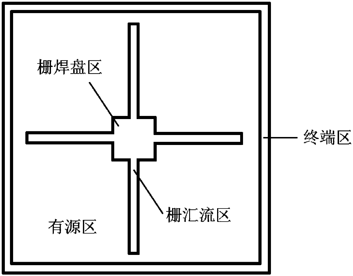
[0048] The schematic diagram of the internal resistance of the gate of the IGBT chip is as follows: Figure 5 As shown, the design of the gate area of ​​the IGBT chip usually also designs the gate resistance, which is called the gate internal resistance. The gate area of ​​the IGBT chip includes the gate pad area and the gate bus bar area; the gate area commonly used in the IGBT chip has a planar type and a trench type. When IGBT chips are used in series, a resistor of about 2-10Ω (ohm) is usually connected in series between the gate pad area a...


PUM


Abstract

The invention relates to a variable grid internal resistance for an IGBT (Insulated Gate Bipolar Transistor) chip. The IGBT chip comprises a grid region; the grid region integrates the switching characteristic of the IGBT chip; the grid region comprises a grid pad region and a grid bus bar region; the grid internal resistance is connected in series between the grid pad region and the grid bus bar region; and the size of the grid internal resistance is between 2ohm and 10ohm. The invention also relates to a design method of the variable grid internal resistance for the IGBT chip. According to the scheme provided by the invention, the grid internal resistance is flexible and variable and has wide application range; and the defect of a fixed grid resistance value in the prior art is improved. By changing a topology of a polycrystal resistance, the regulation on the size of the polycrystal resistance can be implemented. Only by changing one mask (a polycrystal mask), the topology of the polycrystal is changed, the grid internal resistance is regulated and the variable grid internal resistance is conveniently implemented.

Description

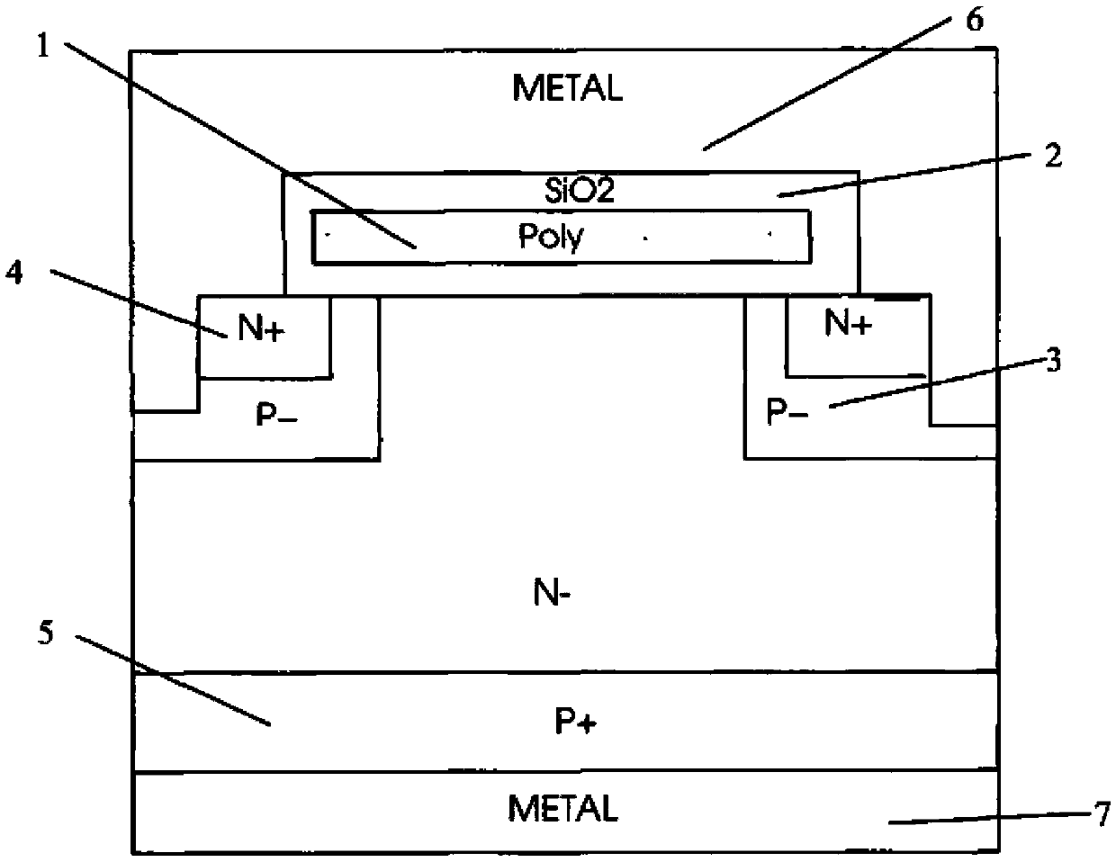
technical field [0001] The invention relates to a gate internal resistance and a manufacturing method thereof, in particular to an IGBT chip variable gate internal resistance and a design method thereof. Background technique [0002] IGBT (Insulated Gate Bipolar Transistor) has the advantages of both unipolar devices and bipolar devices, simple driving circuit, low power consumption and cost of control circuit, low on-state voltage, and low loss of the device itself. It is the future choice for high voltage and high current. Direction of development. [0003] The IGBT is a 3-terminal device, including a front emitter, a gate and a back collector. For the cross-sectional view of the active area of ​​the IGBT chip, see figure 1 . Including a low-concentration N-substrate region; a gate oxide layer 2 on the substrate surface, a polysilicon gate 1 deposited on the gate oxide layer 2; a P-well between the gate oxide layer and the N-substrate region Region 3; N+ region 4 betwe...

Claims


Application Information

Patent Timeline
Patent Type & Authority Patents(China)
IPC IPC(8): H01L29/423H01L29/739H01L21/027H01L21/28H01L21/331
Inventor 刘江高明超赵哿金锐
Owner CHINA ELECTRIC POWER RES INST
Learn More