A Design Method of Te/tm Mode Separator Based on Photonic Crystal Defect Band

A technology of photonic crystal and design method, applied in instruments, light guides, optics, etc., can solve the problems of difficult process, difficult to manufacture, and many polarization crosstalk, and achieve the effect of simple process and low cost

Inactive Publication Date: 2018-06-22
EAST CHINA NORMAL UNIV
View PDF5 Cites 0 Cited by
  • Summary
  • Abstract
  • Description
  • Claims
  • Application Information

AI Technical Summary

Problems solved by technology

The first type is the cross-type, which is characterized by a cross-shaped active area, a relatively simple structure, and low process difficulty, but there are many factors that affect polarization crosstalk, so it is difficult to optimize the structural parameters
The second type is the Y-junction type, which is divided into two types with gap and without gap. It is characterized in that there is only one input port and two output ports. The process is not difficult, but the polarization crosstalk is often large.
The third type is the directional coupler type. This type of device is designed according to the principle of inter-mode coupling, which can achieve very low polarization crosstalk, but the process is difficult and difficult to manufacture.
However, in all these works, they did not try to use the defect bands in the coupled microcavity waveguides to construct TE / TM mode separators, but to use the different wave localization effects of the defect bands to construct TE / TM mode splitters would be show meaningful work

Method used


Image

  • A Design Method of Te/tm Mode Separator Based on Photonic Crystal Defect Band
  • A Design Method of Te/tm Mode Separator Based on Photonic Crystal Defect Band
  • A Design Method of Te/tm Mode Separator Based on Photonic Crystal Defect Band

Examples


Embodiment 1

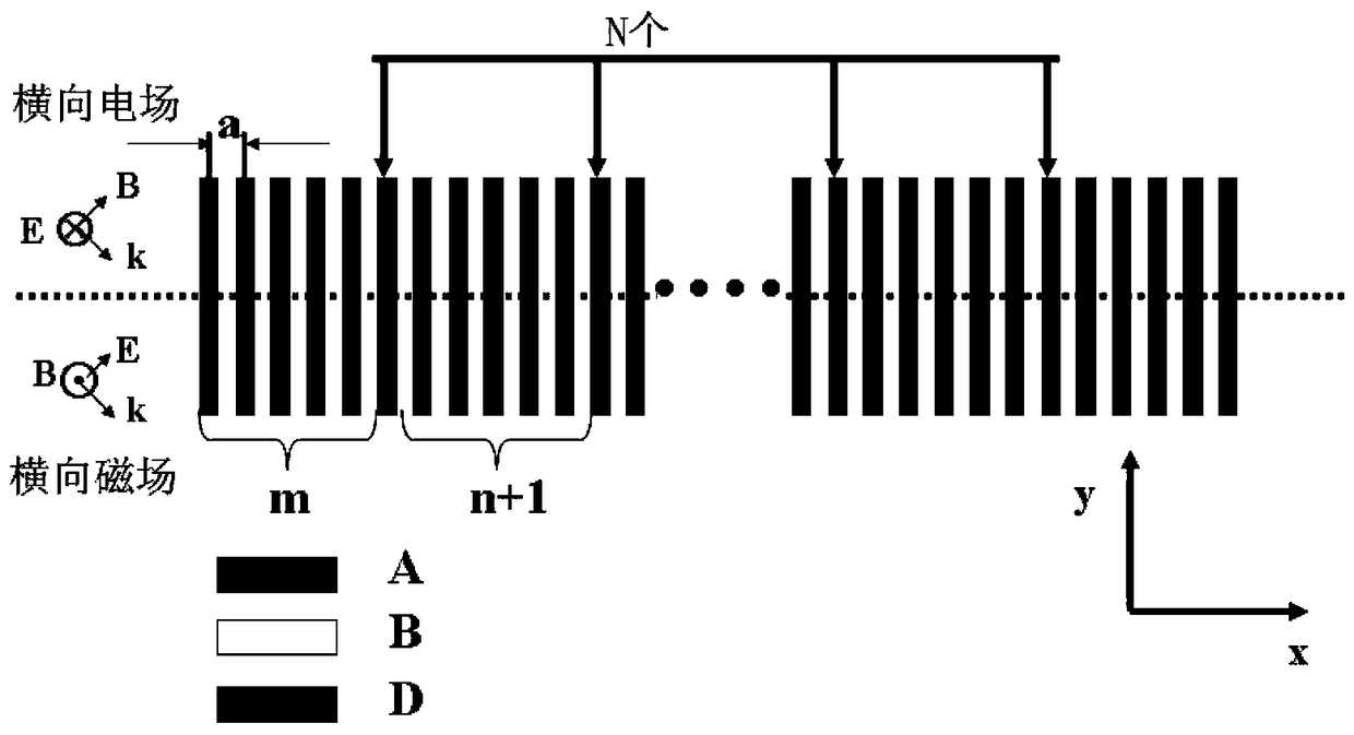
[0025] To illustrate the design method of the TE / TM mode separator, we first illustrate our design process by taking a 1D photonic crystal as an example. like figure 1 As shown, this 1D photonic crystal is constructed of dielectric materials with dielectric constants 1 (air) and 13 (eg silicon), both of which have a normalized thickness of 0.5. In which, N defect layers are periodically introduced to form a coupled microcavity waveguide structure. The dielectric constant of the defect layers can be changed between 1 and 13, and the normalized thickness can also be changed between 0.1 and 0.9.

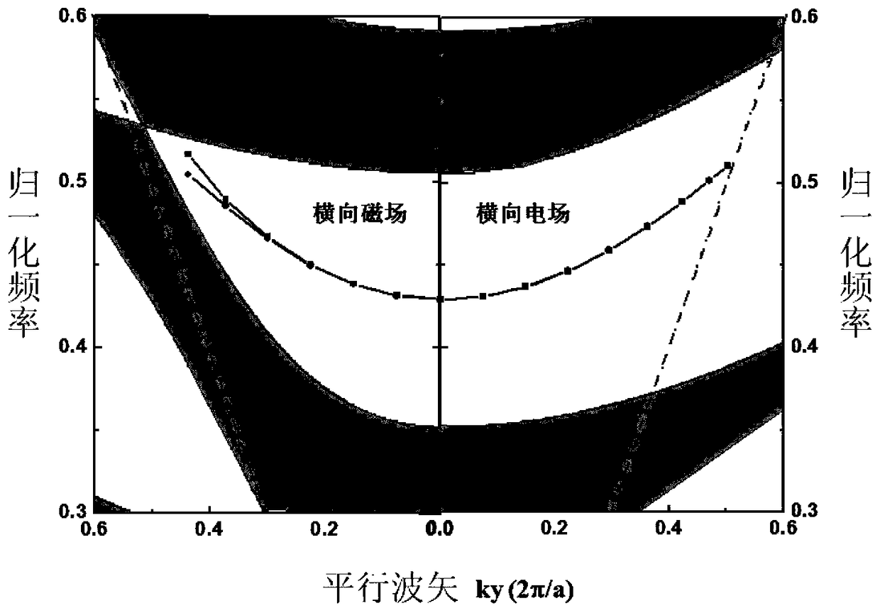
[0026] Here we first choose a case for detailed discussion. For example, we choose the dielectric constant of the defect layer to be 6, its normalized thickness is 0.5, and the number of defect layers is N=10. From the previous calculations, these defect states will form defect bands in the band gap of the photonic crystal. In order to show the nature of the defect band in more detail...

Embodiment 2

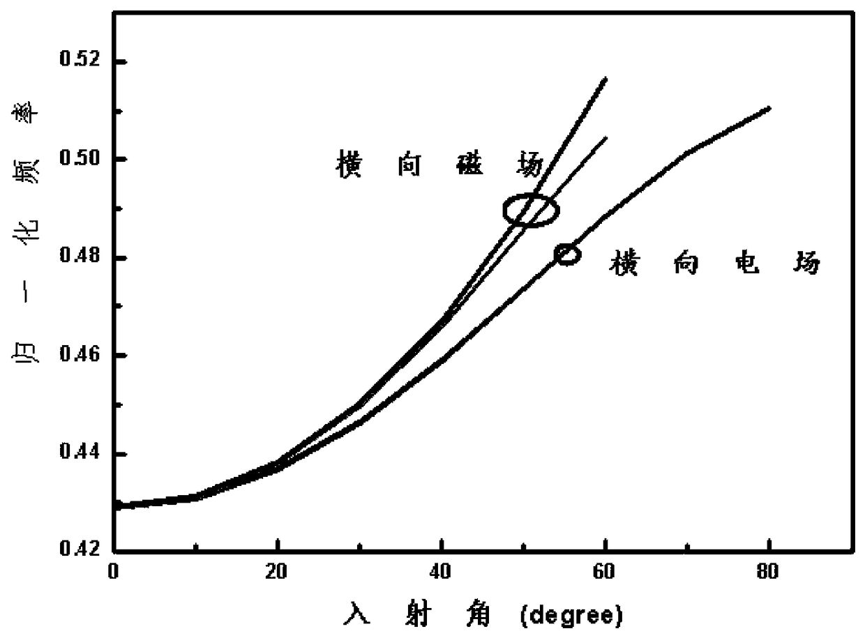
[0028] To illustrate the effect of the parameters of the defect layer on the TE / TM mode separator in more detail, we discuss the properties of different defect layers in detail: when the dielectric constant of the defect layer is 1, similar to the previous discussion process, this coupling can be obtained The minimum splitting angle of the TE / TM defect band of the microcavity waveguide is 17.4. When the dielectric constant of the defect layer is 13, the minimum splitting angle of the TE / TM defect band of this coupled microcavity waveguide is 8.4. Simply put, a defect layer with a low dielectric constant requires a larger incident angle to split the TE / TM defect band. This is because the defect layer with low dielectric constant has poor locality to the electromagnetic field, so that the locality of the electromagnetic field in the TE mode also decreases with the increase of the incident angle, so the defects in the TE and TM modes have the same The variation trend of , for ex...

Embodiment 3

[0030]In order to discuss more completely the application of TE / TM mode separator based on photonic crystal defect band and its special band-like separation effect, we study its physical properties in detail. The transmission of the flat-band structure is realized by adjusting the number of cycles n between defect layers. like Figure 8 Shown is the photonic crystal coupled waveguide transmission spectrum with the number n between defect layers equal to 9, 10 and 11 respectively. It can be found that a wide flat-band result will appear when the number of cycles between defect layers is n=10, enabling broadband transmission, which will be It plays an important role in broadband TE / TM mode separators. In order to be practical, we designed a TE / TM mode separator based on the wavelength of 1550nm in the optical communication band, such as Figure 9 As shown, the electromagnetic wave incident angle is 10 degrees, and the TE / TM mode achieves a good analysis effect. When the incid...


PUM


Abstract

The invention discloses a design method for a transverse electric / transverse magnetic (TE / TM) mode separator based on a photonic crystal imperfect tape. A coupling microcavity wave guiding structure is formed by leading in defect states in a photonic crystal structure periodically, and separation of the TE / TM mode is achieved by controlling the incidence angle of electromagnetic wave. The coupling microcavity wave guiding structure is formed by leading in defect states in the photonic crystal structure periodically, and due to different locality effect of the TE mode and the TM mode in the imperfect tape, waves of the TE mode and the TM mode can be separated under proper incidence angles, the division angle reduces along with increasing of the dielectric constant of the imperfect tape, the division of the two modes can be achieved under the circumference that the incidence angle of the electromagnetic wave is smaller than or equal to 10 degrees, and the design method is suitable for manufacture of the TE / TM mode separator. The design method has large potential application value in the field of physical electronics, optics, materials science, micromotor systems and the like.

Description

technical field [0001] The invention relates to a design method of a novel transverse electric field (TE) / transverse magnetic field (TM) mode separator, in particular to a design method of a TE / TM mode separator based on photonic crystal defect bands. The method is constructed by periodically introducing defect states into a photonic crystal structure, and a TE / TM mode separator is designed by utilizing the variation characteristics of TE and TM defect bands with the incident angle of electromagnetic waves, belonging to the technical fields of optical device systems and optical communication systems. Background technique [0002] TE / TM mode separator is an indispensable part of wavelength division multiplexing technology that does not depend on polarization in coherent optical measurement and optical fiber communication system. Its successful development is used for coherent optical measurement, especially for improving optical fiber communication The capacity of the system ...

Claims


Application Information

Patent Timeline
Patent Type & Authority Patents(China)
IPC IPC(8): G02B6/126G02B6/10
Inventor 徐少辉王连卫
Owner EAST CHINA NORMAL UNIV
Why Eureka
Try Eureka