Substrate for light-emitting element, manufacturing method thereof, and light-emitting device

A light-emitting element and manufacturing method technology, applied in the direction of electrical components, electric solid-state devices, semiconductor devices, etc., can solve the problems of increasing the overall size, difficulty in coping with the miniaturization of LED products, etc., and achieve the effect of improving heat dissipation

Inactive Publication Date: 2016-01-20
PANASONIC INTELLECTUAL PROPERTY MANAGEMENT CO LTD
View PDF9 Cites 0 Cited by
  • Summary
  • Abstract
  • Description
  • Claims
  • Application Information

AI Technical Summary

Problems solved by technology

In other words, as a result, the overall size of the package increases due to the presence of the Zener diode element 270, making it difficult to cope with further miniaturization of LED products.

Method used


Image

  • Substrate for light-emitting element, manufacturing method thereof, and light-emitting device
  • Substrate for light-emitting element, manufacturing method thereof, and light-emitting device
  • Substrate for light-emitting element, manufacturing method thereof, and light-emitting device

Examples


Embodiment Construction

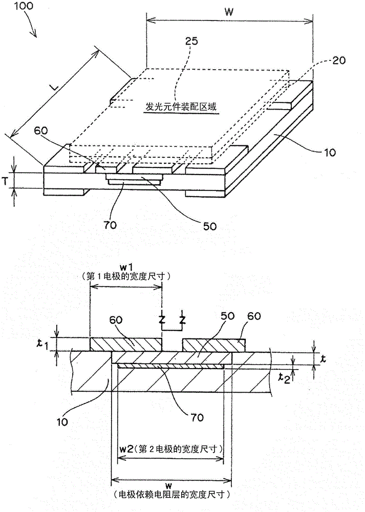
[0070] Hereinafter, the light-emitting element substrate of the present invention and its manufacturing method will be described in detail. In addition, the light-emitting device of the present invention will be described along with this description. In addition, various elements shown in the drawings are only schematically shown for understanding of the present invention, and the size ratio, appearance, and the like may be different from the actual products.

[0071] [Substrate for light-emitting element of the present invention]

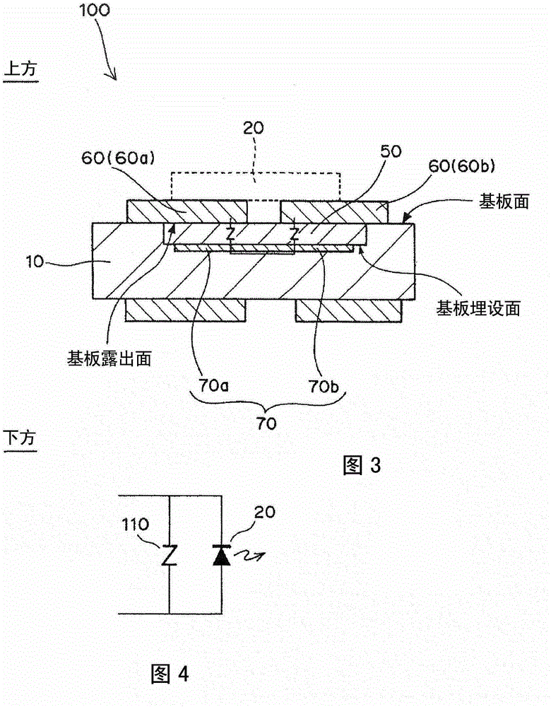
[0072] In the substrate for a light-emitting element of the present invention, a voltage-dependent resistance layer as a protective element is embedded in the substrate area overlapping the mounted light-emitting element. That is, as figure 1 As shown, in the light-emitting element substrate 100 of the present invention, a voltage-dependent resistance layer 50 as a protective element is buried in the light-emitting element mounting area 25 thereof. F...


PUM


Abstract

There is provided a substrate for light-emitting element, including a mounting surface on which a light-emitting element is to be mounted, the mounting surface being one of two opposed main surfaces of the substrate. The substrate of the present invention is provided with a protection element for the light-emitting element, the protection element comprising a voltage-dependent resistive layer embedded in a body of the substrate, and comprising a first electrode and a second electrode each of which is in connection with the voltage-dependent resistive layer wherein the light-emitting element is to be mounted such that it is positioned in an overlapping relation with the voltage-dependent resistive layer.

Description

Technical field [0001] The present invention relates to a substrate for a light-emitting element and a manufacturing method thereof. More specifically, the present invention relates to a substrate for a light-emitting element equipped with a light-emitting diode (hereinafter also referred to as "LED") and a method of manufacturing the substrate. In addition, the present invention also relates to a light-emitting device formed by mounting a light-emitting element on a substrate for a light-emitting element. Background technique [0002] In recent years, LEDs as light sources have the advantages of energy saving and long life, so they are used for various purposes. Especially recently, the luminous efficiency of LEDs has been improved in high light intensity applications, and LEDs have begun to be used for lighting applications. [0003] In the lighting application of white LEDs, the amount of light can be increased by increasing the current applied to the LEDs. However, under suc...

Claims


Application Information

Patent Timeline
Patent Type & Authority Patents(China)
IPC IPC(8): H01L33/62H01L33/64
CPCH01L25/167H01L33/486H01L33/54H01L33/641H01L2924/0002H01L2924/09701H01L2933/0033
Inventor 中谷诚一小川立夫木村一夫濑川茂俊
Owner PANASONIC INTELLECTUAL PROPERTY MANAGEMENT CO LTD
Why Eureka
Try Eureka