


Quick Research
Generate reliable direction feasibility study reports for your R&D in just a few steps.

Technical Q&A
Discover and master advanced knowledge NOW. Basics, ideas, possibilities, all at once.

Find Solutions
As an expert in R&D theories, this can generate solutions to your technical problems instantly.

Evaluate Feasibility
Analyze your overall solution with one click, know your potential R&D risks in advance.

Monitor Landscape
Get weekly tech updates, stay abreast of the latest tech innovations and key insights.
Threshold voltage degradation measuring circuit
A threshold voltage and measurement circuit technology, applied in the direction of measuring electrical variables, measuring current/voltage, measuring devices, etc., can solve the problems of complex threshold voltage degradation measurement process, threshold voltage degradation, high equipment cost, etc., to achieve simple structure and save time , the effect of convenient operation
- Summary
- Abstract
- Description
- Claims
- Application Information
AI Technical Summary
Problems solved by technology
Method used
Image

Examples
Embodiment 1
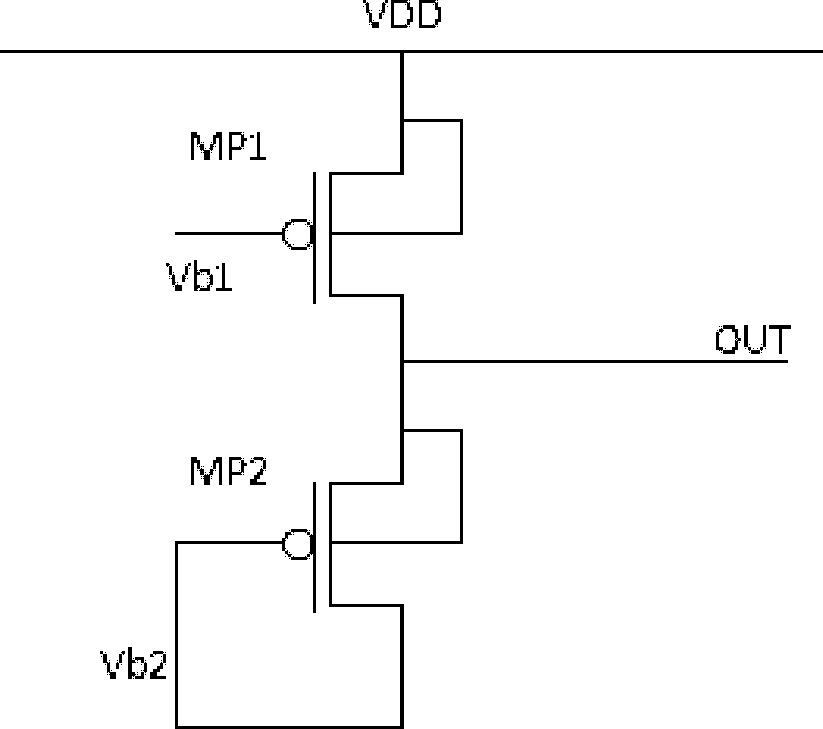
[0023] In Embodiment 1 of FIG. 1( a ), two PMOS transistors connected in series are taken as an example for illustration. Wherein, the first PMOS transistor MP1 is the tube under test, and the purpose of the circuit of the present invention is to determine the degradation of the threshold voltage of the tube under test MP1 through the voltage change of the output terminal OUT during normal operation.
[0024] Specifically, the gate of the first PMOS transistor MP1 is connected to the first DC voltage Vb1, the source and the substrate are simultaneously connected to the source voltage (in Embodiment 1, the source voltage is the power supply voltage VDD), and the drain is connected to the output terminal OUT; The gate and drain of the second PMOS transistor MP2 are connected to the second DC voltage Vb2 at the same time, and the source and substrate are connected to the output terminal OUT at the same time.
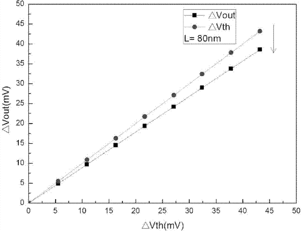
[0025] In the present invention, in order to enable the circuit to rea...
Embodiment 2
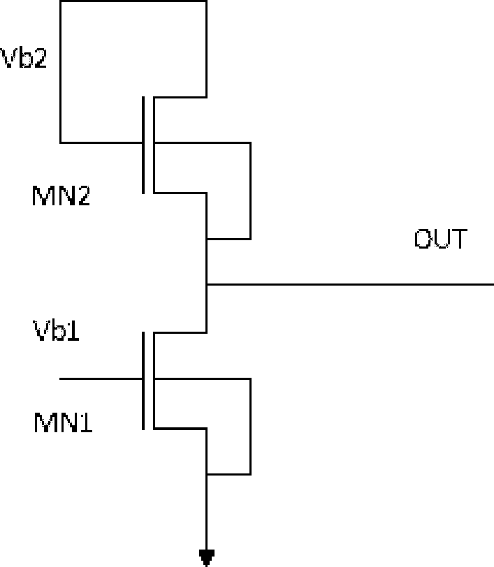
[0036] In Embodiment 2 of FIG. 1( b ), two NMOS transistors connected in series are taken as an example for illustration. Wherein, the first NMOS transistor MN1 is the tube under test, and the purpose of the circuit of the present invention is to determine the threshold voltage degradation of the tube under test MN1 through the voltage change of the output terminal OUT during normal operation.
[0037] Specifically, the gate of the first NMOS transistor MN1 is connected to the first DC voltage Vb1, the source and substrate are grounded at the same time, and the drain is connected to the output terminal OUT; the gate and drain of the second NMOS transistor MN2 are connected to the second DC voltage at the same time Vb2, the source and the substrate are connected to the output terminal OUT at the same time.
[0038] In the present invention, in order to enable the circuit to realize the function of testing the degradation of the threshold voltage of the first NMOS transistor, it...
PUM
 Abstract
Description
Claims
Application Information
 - R&D Engineer
- R&D Manager
- IP Professional
- Industry Leading Data Capabilities
- Powerful AI technology
- Patent DNA Extraction
Browse by: Latest US Patents, China's latest patents, Technical Efficacy Thesaurus, Application Domain, Technology Topic, Popular Technical Reports.
© 2024 PatSnap. All rights reserved.Legal|Privacy policy|Modern Slavery Act Transparency Statement|Sitemap|About US| Contact US: help@patsnap.com