
Laser processing of display components for electronic devices

An electronic equipment and laser technology, applied in welding equipment, laser welding equipment, metal processing equipment, etc., can solve problems such as difficulty in maintaining manufacturing tolerances

Inactive Publication Date: 2012-08-08
APPLE INC
View PDF8 Cites 17 Cited by
  • Summary
  • Abstract
  • Description
  • Claims
  • Application Information

AI Technical Summary

Problems solved by technology

However, it can be difficult to maintain desired manufacturing tolerances during the die-cutting and lamination processes in the display manufacturing process

Method used


Image

  • Laser processing of display components for electronic devices
  • Laser processing of display components for electronic devices
  • Laser processing of display components for electronic devices

Examples


Embodiment Construction

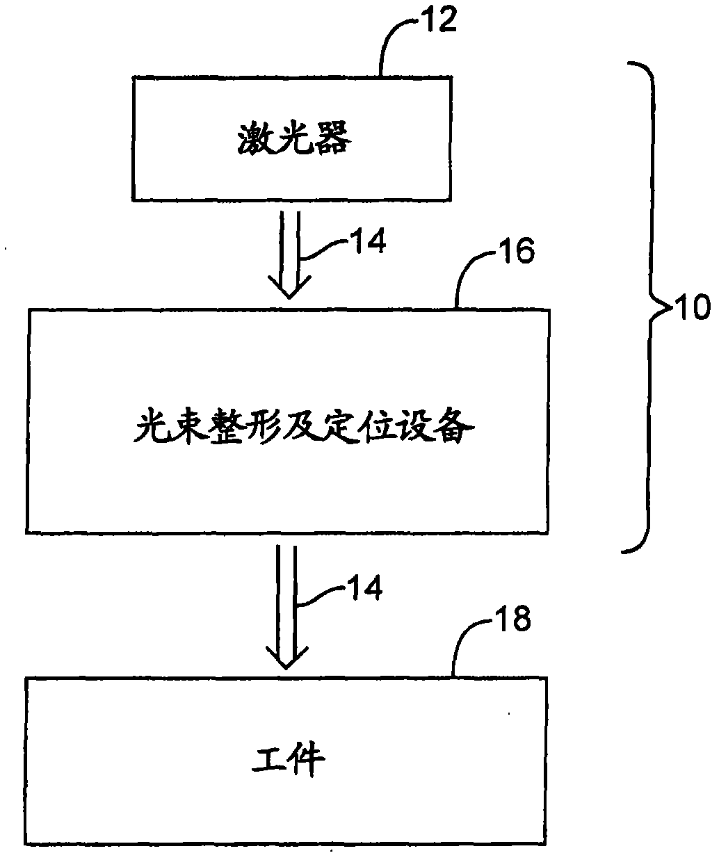
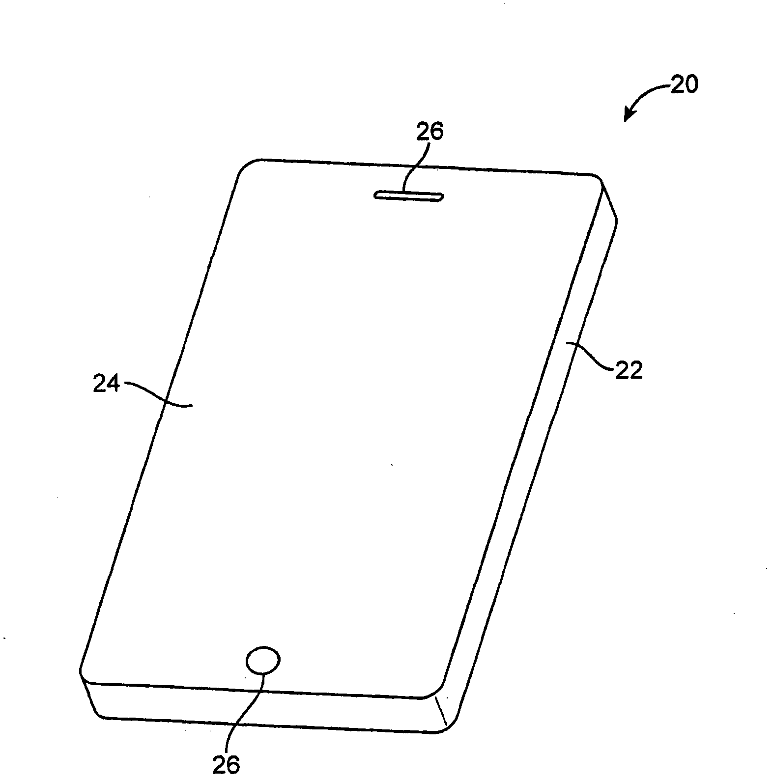
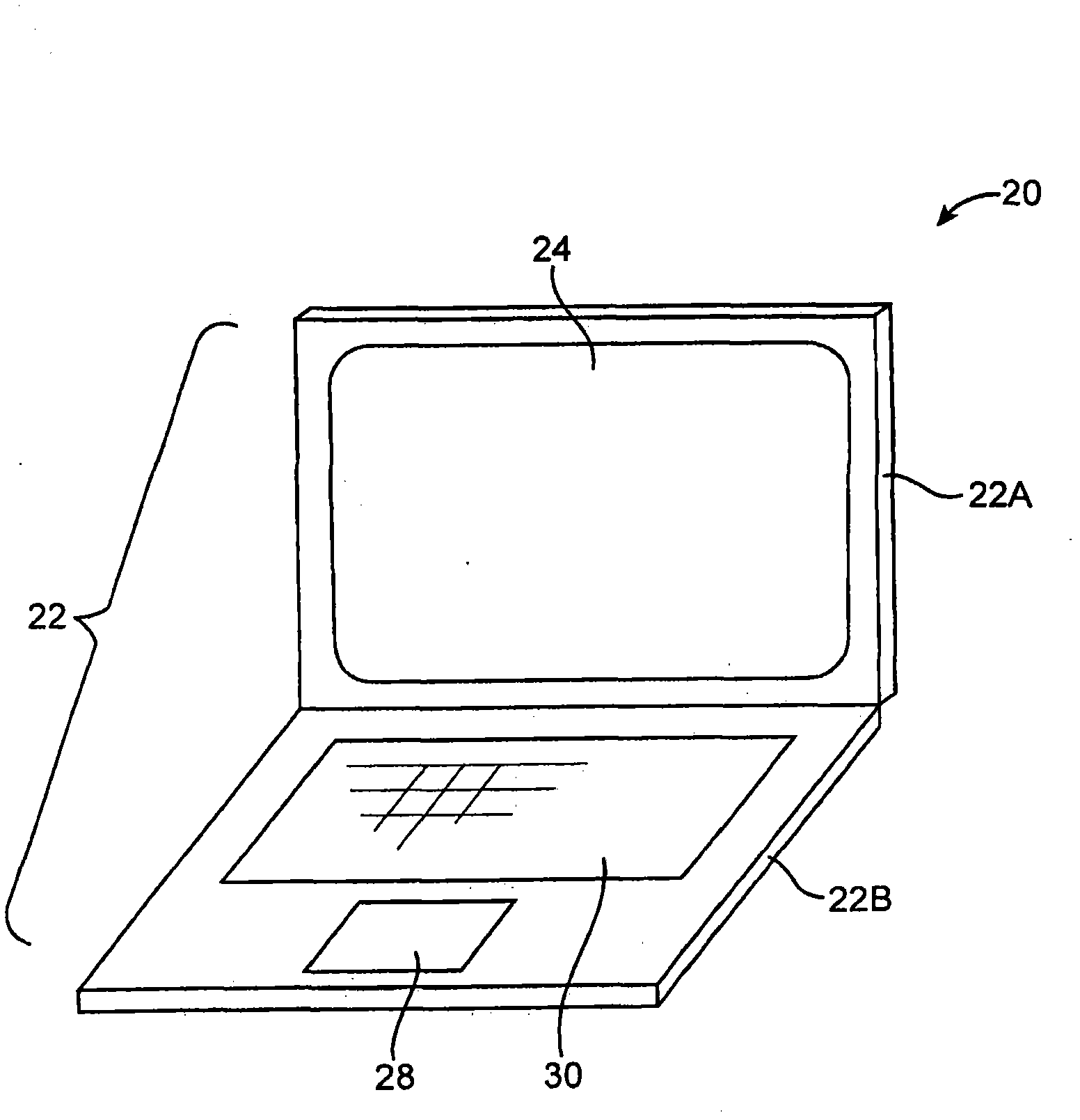
[0032] Displays are widely used in electronic devices. For example, displays may be used in computer monitors, laptops, media players, cellular telephones and other handheld devices, tablet computers, televisions, and other devices. Displays may be based on plasma technology, organic light emitting diode technology, liquid crystal structures, etc.

[0033] Displays typically include layers of materials. For example, a liquid crystal display may include a color filter array layer with color filter elements, a thin film transistor layer with thin film transistors for controlling the application of an electric field to the liquid crystal image pixels. A cover sheet layer can be used to cover the display. The cover sheet layer and other display layers such as color filter array layers and thin film transistor layers typically can be formed from glass, but can also be formed from other substrate materials such as polymers if desired.

[0034] Typically there are multiple additio...


PUM

PropertyMeasurementUnit
Diameteraaaaaaaaaa
Horizontal sizeaaaaaaaaaa

Abstract

Electronic devices may be provided with display structures such as glass and polymer layers in a liquid crystal display. The glass layers may serve as substrates for components such as a color filter layer and thin-film transistor layer. The polymer layers may include films such as a polarizer film and other optical films. During fabrication of a display, the polymer layers and glass layers may be laminated to one another. Portions of the polymer layers may extend past the edges of the glass layers. Laser cutting techniques may be used to trim away excess portions of the polymer layer that do not overlap underlying portions of the glass layers. Laser cutting may involve application of an adjustable infrared laser beam.

Description

technical field [0001] The present disclosure relates generally to fabrication techniques for electronic devices, and more particularly to the application of laser processing techniques in fabricating electronic device structures, such as display structures. Background technique [0002] Displays are widely used in electronic devices to display images. Displays, such as liquid crystal displays, display images by controlling liquid crystal material associated with an array of image pixels. A typical liquid crystal display has a color filter layer and a thin film transistor layer with a liquid crystal material in between. Polarizer layers may be formed on upper and lower surfaces of the color filter layer and the thin film transistor layer. Other optical films may also be present. [0003] As part of the process of forming liquid crystal displays, sheets of polarizing and other optical films must be cut to size. For example, when forming a display for a handheld device suc...

Claims


Application Information

Patent Timeline
IPC IPC(8): B23K26/38G09F9/35
CPCB23K26/38G09F9/35B23K2103/42B23K2103/50Y10T156/108B29C2793/0027Y10T156/1348B32B38/105B23K26/0876B23K26/103B23K26/402
Inventor 齐军W·H·弗王晨辉林宽颖N·K·古普塔V·H·因
Owner APPLE INC
Learn More