A uhf_rfid tag and antenna with a multimedia structure
A multi-media and antenna technology, applied in the field of RFID (Radio Frequency Identification) tags, to achieve the effect of good Q value performance, reduced loss, and low loss tangent value
- Summary
- Abstract
- Description
- Claims
- Application Information
AI Technical Summary
Problems solved by technology
Method used
Image
Examples
Embodiment 1
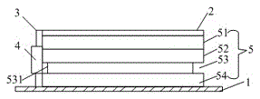
[0025] see figure 1 , which is a schematic cross-sectional diagram of a UHF_RFID tag with a multi-media structure. It includes antenna and IC chip 4 . The antenna further includes a dielectric substrate 5, one side of the dielectric substrate 5 is provided with a ground layer 1, and the corresponding surface is provided with a radiation electrode layer 2, and the radiation electrode layer 2 is connected to the IC chip 4 through a microstrip line or a probe 3, (mainly Refers to that the radiation electrode layer 2 is connected to the RF port of the IC chip 4 through a microstrip line or probe 3), the ground layer 1 is directly connected to the GND port of the IC chip 4 through a section of metal layer, and the dielectric substrate 5 includes There are at least two dielectric layers, the dielectric constants of the two adjacent dielectric layers are different, and the dielectric of the dielectric layer is a non-metallic material.
[0026] exist figure 1 Among them, the dielec...
Embodiment 2
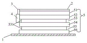
[0034] see figure 2 , which is a schematic cross-sectional schematic diagram of the second type of UHF_RFID tag with a multi-media structure.
[0035] The dielectric substrate can be composed of two layers or multiple dielectric layers. For example, the epoxy board layer is connected to the air layer to form a group, and the dielectric substrate can include multiple groups 52, 53, 54, 55, 56.
Embodiment 3
[0037] The invention provides an antenna, comprising a dielectric substrate, a ground layer is arranged on one side of the dielectric substrate, and a radiation electrode layer is arranged on the corresponding surface, and the radiation electrode layer is connected to an external IC chip through a microstrip line or a probe. The dielectric substrate includes at least two dielectric layers, the dielectric constants of the two adjacent dielectric layers are different, and the dielectric of the dielectric layer is non-metallic material.
[0038] The dielectric layer includes an air layer, the air layer includes a bracket, and the air layer is connected to the ground layer or other dielectric layers through the bracket.
[0039] The dielectric substrate includes multiple dielectric layers.
[0040] The medium layer can be epoxy board layer, plastic layer and air layer appearing alternately.
[0041] A manufacturing process of a UHF_RFID anti-metal tag with a multi-media structure...
PUM
 Abstract
Description
Claims
Application Information
 - R&D
- Intellectual Property
- Life Sciences
- Materials
- Tech Scout
- Unparalleled Data Quality
- Higher Quality Content
- 60% Fewer Hallucinations
Browse by: Latest US Patents, China's latest patents, Technical Efficacy Thesaurus, Application Domain, Technology Topic, Popular Technical Reports.
© 2025 PatSnap. All rights reserved.Legal|Privacy policy|Modern Slavery Act Transparency Statement|Sitemap|About US| Contact US: help@patsnap.com


