
FPGA (field programmable gate array) interconnection line time-delay acquiring method and system utilizing same

An acquisition method and acquisition system technology, which is applied in the field of FPGA interconnect line delay acquisition, can solve the problems of heavy workload and inaccurate simulation, and achieve the effect of high accuracy and easy acquisition

Inactive Publication Date: 2012-07-04
SHENZHEN STATE MICROELECTRONICS CO LTD
View PDF4 Cites 5 Cited by
  • Summary
  • Abstract
  • Description
  • Claims
  • Application Information

AI Technical Summary

Problems solved by technology

These two methods have certain limitations. The Elmore delay acquisition method is not accurate enough because it uses a simplified RC network.
The method of testing is to repeatedly use some units and interconnection lines by continuously writing the design, but due to the large variety of interconnection lines, the workload of using this method is very large

Method used


Image

  • FPGA (field programmable gate array) interconnection line time-delay acquiring method and system utilizing same
  • FPGA (field programmable gate array) interconnection line time-delay acquiring method and system utilizing same
  • FPGA (field programmable gate array) interconnection line time-delay acquiring method and system utilizing same

Examples


Embodiment Construction

[0024] combine figure 2 , image 3 , Figure 4 with Figure 5 , to further describe the embodiments of the present invention.

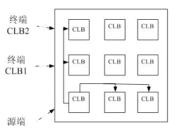
[0025] Generally speaking, the interconnection line includes a programmable configuration selector (MUX), an inverter (inverter) on the line, and a physical line. Most FPGAs adopt a programmable interconnection line model of hierarchical interconnection. In this model, there are usually three types of connections in the wiring channel, namely, the short line (Short Line) of the adjacent high-speed interconnection level, and the local connection line. For Dividable Long Line at the level and Long Line at the global level, the configuration selector acts as a switch for connecting between different lines.

[0026] The interconnection delay is mainly affected by the structure, drive and load of the interconnection. The drivers and loads of the three types of interconnections, short-term, divisible long-term, and long-term, are different. Therefore, ...


PUM


Abstract

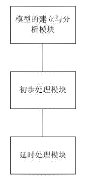
The invention provides an FPGA (field programmable gate array) interconnection line time-delay acquiring method and a system utilizing the same. The FPGA interconnection line time-delay acquiring method includes: the model building and analyzing step: dividing an interconnection line of the FPGA into a plurality of models, determining the number of varied paths caused by the number of varied loads of each model; the initial processing step: obtaining time delay of each path by a net list extracted by a layout according to variation of the number of loads and filling the time delay parameters of the models into a database; the time delay processing step: obtaining interconnection line models by searching the database during layout arranging and wiring, then calling the time delay parameters of the corresponding model to acquire the total time delay of the integral interconnection line by means of fitting of numerical values.

Description

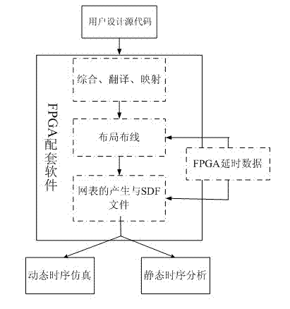
technical field [0001] The invention relates to a method and a system for acquiring the time delay of an FPGA interconnection line. Background technique [0002] In today's Field Programmable Gate Array (FPGA) field, the development and application steps of the chip function in the prior art are: the user provides the design source code -> synthesize each circuit module of the chip according to the design idea of ​​the design source code, Translation, mapping, and placement and routing (placement and routing is to lay out the design of the source code to connect it to a specific circuit function module in the FPGA) -> get configuration information -> download the configuration information to the corresponding FPGA , specific functions can be realized. In this process, it is necessary to carry out reasonable layout and wiring to meet the requirements of logic and timing, and obtain the highest operating frequency of the chip according to the results of layout and wi...

Claims


Application Information

Patent Timeline
Patent Type & Authority Applications(China)
IPC IPC(8): G06F17/50
Inventor 包朝伟赵多华袁梅
Owner SHENZHEN STATE MICROELECTRONICS CO LTD
Learn More