In-chip power conversion control circuit of system chip based on system bus

A system bus and power conversion technology, which is applied in control/regulation systems, regulation of electrical variables, instruments, etc., can solve problems such as reducing system power supply voltage, and achieve the effect of simplified structure, simple structure, and simple circuit structure

Inactive Publication Date: 2014-02-05
SOUTHEAST UNIV
View PDF5 Cites 0 Cited by
  • Summary
  • Abstract
  • Description
  • Claims
  • Application Information

AI Technical Summary

Problems solved by technology

In actual use, the workload of system components changes dynamically over time. Dynamic power management switches components with lighter loads to an operating state with lower power consumption. Although the performance is lower, it is in advance to meet the performance requirements. Dynamically reduce the system power supply voltage, thereby reducing system power consumption

Method used


Image

  • In-chip power conversion control circuit of system chip based on system bus
  • In-chip power conversion control circuit of system chip based on system bus
  • In-chip power conversion control circuit of system chip based on system bus

Examples


Embodiment Construction

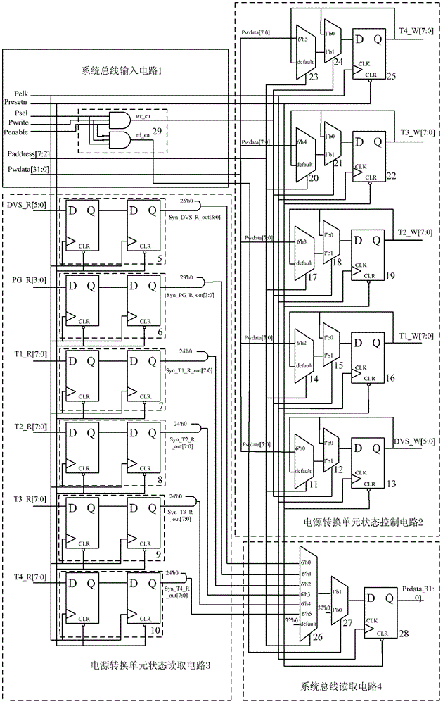
[0021] A system chip on-chip power conversion control circuit based on a system bus, characterized in that it includes a system bus input circuit 1, a power conversion unit state control circuit 2, a power conversion unit state reading circuit 3 and a system bus reading circuit 4,

[0022] The system bus input circuit 1 includes two AND gates 29 with 3 input terminals, wherein the 3 input terminals of the AND gate receive input signals Psel, Pwrite and Penable, generate a wr_en signal for controlling the write operation, and output it to the power conversion unit state control circuit 2 , the 3 input terminals of the other AND gate receive the reverse signal of Penable and Pwrite and the Psel signal, and generate the rd_en signal for controlling the read operation and output it to the system bus read circuit 4;

[0023]The power conversion unit state control circuit 2 includes a DVS_W data write circuit and at least two T_W data write circuits, and the DVS_W data write circuit ...


PUM


Abstract

The invention relates to an in-chip power conversion control circuit of a system chip based on system bus. The in-chip power conversion control circuit comprises a system bus input circuit, a power conversion unit state control circuit, a power conversion unit state reading circuit, and a system bus reading circuit, wherein the system bus input circuit includes a 3-input and gate for generating a write and read control signal; the power conversion unit state control circuit includes data paths for writing data into a power conversion unit, each path including two stages of data selectors and one stage of trigger; the power conversion unit state reading circuit includes data paths for reading state data from a power conversion unit, each path including two stages of triggers; and the system bus reading circuit includes two stages of selectors and one stage of trigger, and is used for reading state data of the power conversion unit. According to the scheme, the in-chip power conversion control circuit has simple structure, and can directly control an in-chip power management system composed of a plurality of power conversion units through the system bus, thereby meeting the requirement of low-power-consumption system chip design for different voltages.

Description

technical field [0001] The invention relates to a power management unit circuit (power management), which belongs to the design of an integrated circuit and belongs to the field of electronic technology, in particular to a system bus-based on-chip power conversion control circuit for a system chip. Background technique [0002] Power management (power management) is a power management technology that is widely used in power consumption control of portable electronic devices, mobile communication devices, and network devices. In actual use, the workload of system components changes dynamically over time. Dynamic power management switches components with lighter loads to a lower power consumption operating state. Although the performance is lower, it is in advance to meet the performance. Dynamically reduce the system power supply voltage, thereby reducing system power consumption. [0003] The classification of existing power management units (power management) commonly incl...

Claims


Application Information

Patent Timeline
Patent Type & Authority Patents(China)
IPC IPC(8): G05F1/46
Inventor 徐申孙大鹰徐玉珉孙伟锋陆生礼时龙兴
Owner SOUTHEAST UNIV
Why Eureka
Try Eureka