Manufacturing method of planar optical waveguide device with grating structure
A planar optical waveguide and groove technology, applied in optical waveguides, light guides, optics, etc., can solve the problem that the knowledge of the lithography process has not been fully accumulated, and achieve the effects of easy processing accuracy and easy control.
- Summary
- Abstract
- Description
- Claims
- Application Information
AI Technical Summary
Problems solved by technology
Method used
Image

Examples
no. 1 approach
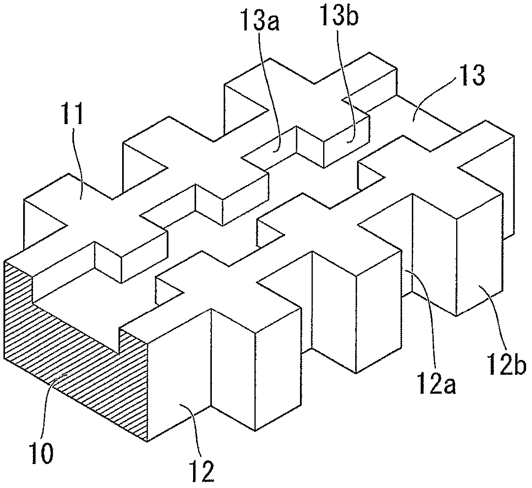
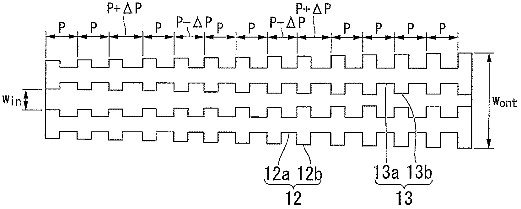
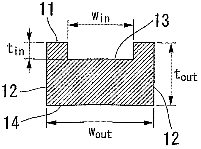
[0163] A planar light waveguide device according to a first embodiment of the present invention is schematically shown in Figures 1A to 1C middle. Figure 1A is a perspective view showing a part of the core wire 10 of the optical waveguide, Figure 1B is a top view showing the same part of the core wire 10, Figure 1C is a cross-sectional view showing a planar optical waveguide device. also, Figure 16 A perspective view of a planar optical waveguide is shown in . At the same time, in Figure 1C In , reference numerals 12 and 13 are used to indicate the side wall and groove structure of the core wire 10 without distinguishing Figure 1A with 1B Concaves (recesses) 12a and 13a and protrusions (convexes) 12b and 13b.
[0164] In this planar optical waveguide device, an optical waveguide is formed on a substrate 15 . The optical waveguide has a lower cladding layer 16 formed on a substrate 15 , a core wire 10 formed on the lower cladding layer 16 , and an upper cladding ...
no. 1 example
[0307] like Figures 1A to 1C As shown, a dispersion compensator for a polarity-dependent planar optical waveguide is designed and fabricated, in which the core wire is formed of silicon nitride (SiN) and the cladding layer is made of silica glass (SiO 2 ) is formed, and the dispersion compensator has a grating structure on the core sidewall and upper portion of the optical waveguide.
[0308] according to Figure 1C The structural design of the cross-sectional structure of the optical waveguide, and as Figure 5 Shown to calculate W in and W out Relationship to the effective refractive index of the optical waveguide.
[0309] Then, design the raster pattern. The designed center frequency is 188.4THz. That is, the designed center wavelength is 1591.255 nm. The group delay dispersion and dispersion slope of a single-mode dispersion-shifted fiber (DSF) with a length of 100 km is specified in ITU-T G.653 with 100 GHz channel spacing in the L-band, and is to be object of c...
Embodiment approach
[0350] Figure 36 is a sectional view showing a planar optical waveguide device according to a third embodiment of the present invention. A dual-core structure including inner cores 21 and 22 for changing optical characteristics and an outer core 24 for solving polarization dependence of optical properties is suitable for the planar optical waveguide device 20 .
[0351] This twin wire structure exists on the lower cladding layer 26 formed on the substrate 25 . The upper part and both sides of the composite core wire are covered with an upper cladding layer 27 . The upper cladding layer 27 and the lower cladding layer 26 are formed of a material having a refractive index lower than the average refractive index of the twin-wire structure. The material of the lower cladding layer 26 and the material of the upper cladding layer 27 may be the same or different.
[0352] The inner core wires 21 and 22 are divided into two by a central gap 23 interposed therebetween. The inner c...
PUM
| Property | Measurement | Unit |
|---|---|---|
| wavelength | aaaaa | aaaaa |
| wavelength | aaaaa | aaaaa |
Abstract
Description
Claims
Application Information
 - R&D
- Intellectual Property
- Life Sciences
- Materials
- Tech Scout
- Unparalleled Data Quality
- Higher Quality Content
- 60% Fewer Hallucinations
Browse by: Latest US Patents, China's latest patents, Technical Efficacy Thesaurus, Application Domain, Technology Topic, Popular Technical Reports.
© 2025 PatSnap. All rights reserved.Legal|Privacy policy|Modern Slavery Act Transparency Statement|Sitemap|About US| Contact US: help@patsnap.com