
Deposited film formation device and deposited film formation method

A technology for depositing films and electrodes, applied in gaseous chemical plating, coatings, electrical components, etc., can solve problems such as uneven temperature distribution, and achieve the effect of suppressing the temperature rise of the second electrode

Inactive Publication Date: 2012-05-30
KYOCERA CORP
View PDF7 Cites 0 Cited by
  • Summary
  • Abstract
  • Description
  • Claims
  • Application Information

AI Technical Summary

Problems solved by technology

This is mainly caused by the fact that the in-plane temperature distribution of the cathode electrode is easily uneven.

Method used


Image

  • Deposited film formation device and deposited film formation method
  • Deposited film formation device and deposited film formation method
  • Deposited film formation device and deposited film formation method

Examples


no. 1 example

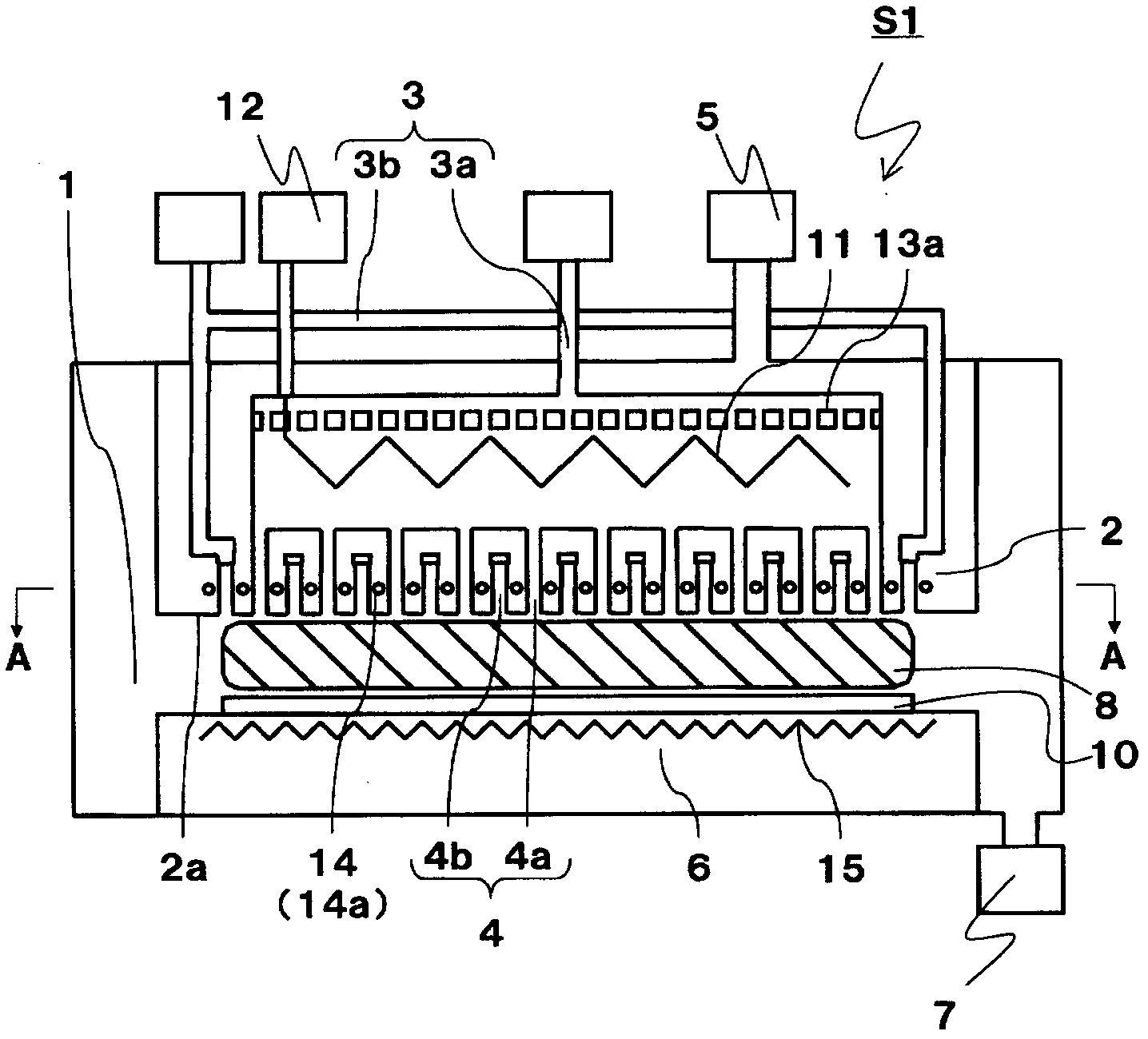
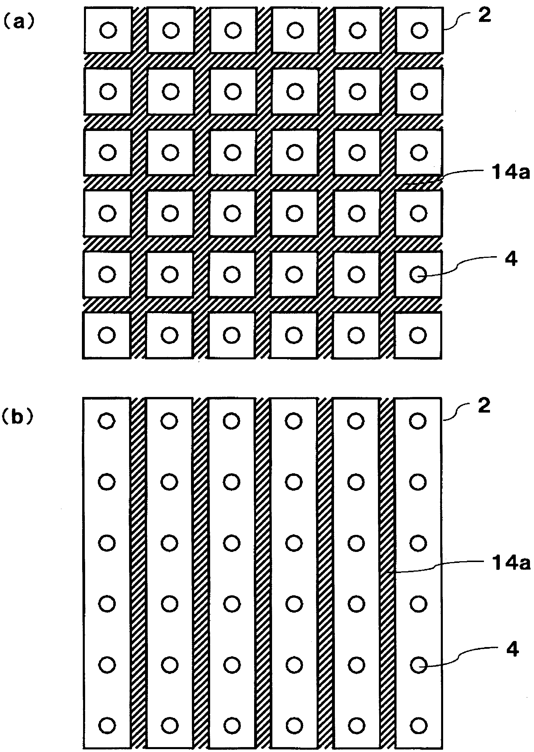
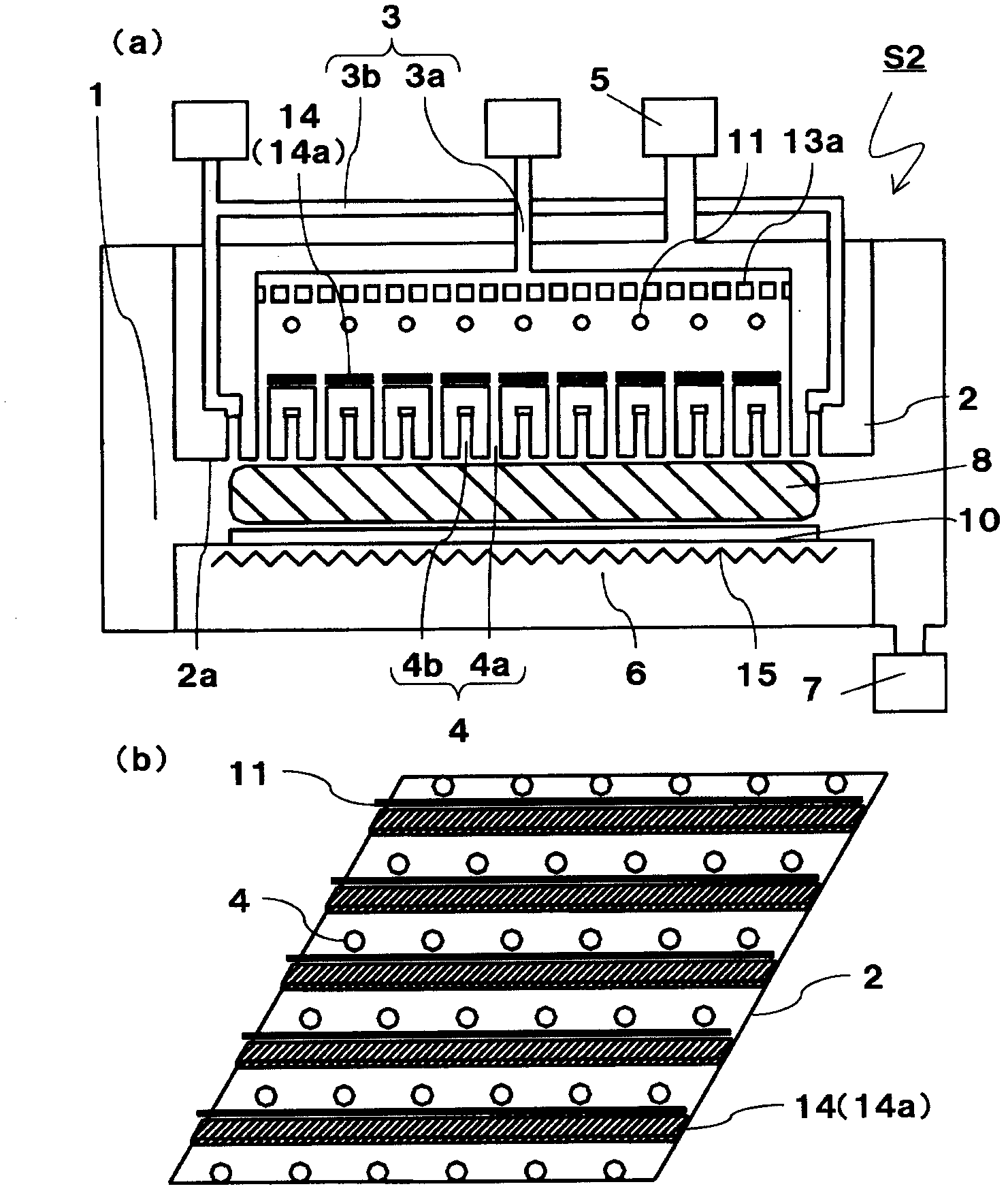
[0135] Next, compare the following three situations: the inside of the second electrode 2 made of stainless steel is provided with a cooling mechanism 14, and the cooling mechanism 14 has a situation in which the refrigerant is a lattice-shaped refrigerant path of silicone oil; 2, a cooling mechanism 14 is set inside the first electrode 6, and a base material heat dissipation unit 16 is set inside the first electrode 6, and the base material heat dissipation unit 16 has a case where the refrigerant is a grid-like refrigerant path of silicone oil; the cooling mechanism 14 and the base material dissipate heat Unit 16 is not set.

[0136] As the deposited film forming apparatus, an apparatus is prepared which is composed of the second electrode 2 and the first electrode 6, wherein the second electrode 2 has a function for supplying H 2 The first supply part 4a for gas (first raw material gas) and for supplying SiH 4 The second supply part 4b of gas (second raw material gas), the...

no. 2 example

[0144] Under the above-mentioned conditions A to E, respectively, on the substrate 10 made of glass having a transparent conductive film on the surface, a photoelectric conversion layer composed of an amorphous silicon film and having a pin junction is formed in order from bottom to top. The microcrystalline silicon film has a photoelectric conversion layer with a pin junction and a back electrode, thereby forming a double-layer thin-film solar cell, and comparing the power generation efficiency. At this time, the film thickness of the i-type amorphous silicon film is The film thickness of the i-type microcrystalline silicon film was 2.8 μm.

[0145] The photoelectric conversion layer made of an amorphous silicon film and the p-type and n-type microcrystalline silicon films were formed using a parallel plate type plasma CVD apparatus. In addition, the i-type microcrystalline silicon film was formed using a deposition film forming apparatus for heating a catalytic body under ...


PUM


Abstract

Disclosed is a deposited film formation device that, in order to form a high quality film without the occurrence of surface unevenness in the quality of the film, is equipped with a chamber; a first electrode that is disposed within said chamber; a second electrode that is disposed within the aforementioned chamber at a prescribed distance from the first electrode, and that is provided with a plurality of supply units that supply a source gas; an introduction path through which the source gas is introduced, that is connected to the aforementioned supply units; a heating means that is disposed in said introduction path; and cooling mechanisms that cool the aforementioned second electrode.

Description

technical field [0001] The present invention relates to a deposited film forming apparatus and a deposited film forming method for forming a deposited film such as thin film silicon (Si) on a substrate. Background technique [0002] A conventional deposited film forming apparatus is provided with: a chamber; a gas introduction path for introducing a source gas into the chamber; and a pair of electrodes arranged in the chamber. And, a substrate on which a deposited film is to be formed is placed on one of the pair of electrodes. The other electrode of the pair of electrodes is connected to a high-frequency power supply for applying high-frequency power to the electrode. [0003] Here, in the space between the pair of electrodes, the applied high-frequency power is used as dissociation energy to decompose and activate the raw material gas to generate various reactive species. And, some of these active ingredients are deposited on the substrate to form a film. [0004] As su...

Claims


Application Information

Patent Timeline
IPC IPC(8): C23C16/455H01L31/04
CPCH01L31/18C23C16/455H01L31/04C23C16/5096
Inventor 伊藤宪和稻叶真一郎松居宏史新乐浩一郎
Owner KYOCERA CORP
Learn More