
Low grid-drain capacitance grooved metal oxide silicon (MOS) device and manufacturing method thereof

A technology of MOS devices and leakage capacitors, which is applied in semiconductor/solid-state device manufacturing, electrical components, semiconductor devices, etc., can solve the problem of poor Cgd/Cgs consistency, affecting device performance and device reliability, and affecting the ability of devices to suppress false turn-on and other issues, to achieve the effect of suppressing false turn-on ability, improving device performance and reliability, and low cost

Active Publication Date: 2014-01-15
SUZHOU SILIKRON SEMICON CO LTD
View PDF6 Cites 0 Cited by
  • Summary
  • Abstract
  • Description
  • Claims
  • Application Information

AI Technical Summary

Problems solved by technology

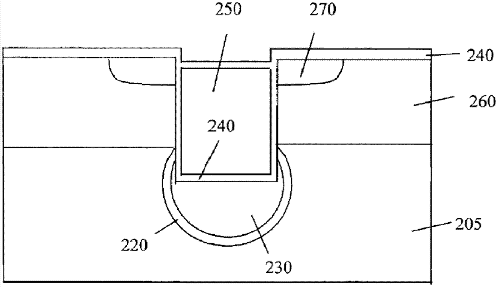
[0005] 1. The gate oxide layer at the bottom of the gate trench is oxidized and grown from conductive polysilicon filled in the circular hole. The density and thickness uniformity of the oxide layer are worse than those grown on single crystal silicon, which affects device performance and Device reliability;
[0006] 2. The gate trench etching adopts the time modulation method. The depth of the gate trench is determined by the etching amount of the conductive polysilicon filled in the circular hole. The etching process is difficult to control and the consistency of the gate trench depth is low.
Although due to the existence of the circular hole structure, the inconsistent gate trench depth will not cause Cgd inconsistency, but it will cause Cgs difference, resulting in poor consistency of Cgd / Cgs and affecting the device's ability to suppress false turn-on

Method used


Image

  • Low grid-drain capacitance grooved metal oxide silicon (MOS) device and manufacturing method thereof
  • Low grid-drain capacitance grooved metal oxide silicon (MOS) device and manufacturing method thereof
  • Low grid-drain capacitance grooved metal oxide silicon (MOS) device and manufacturing method thereof

Examples


Embodiment

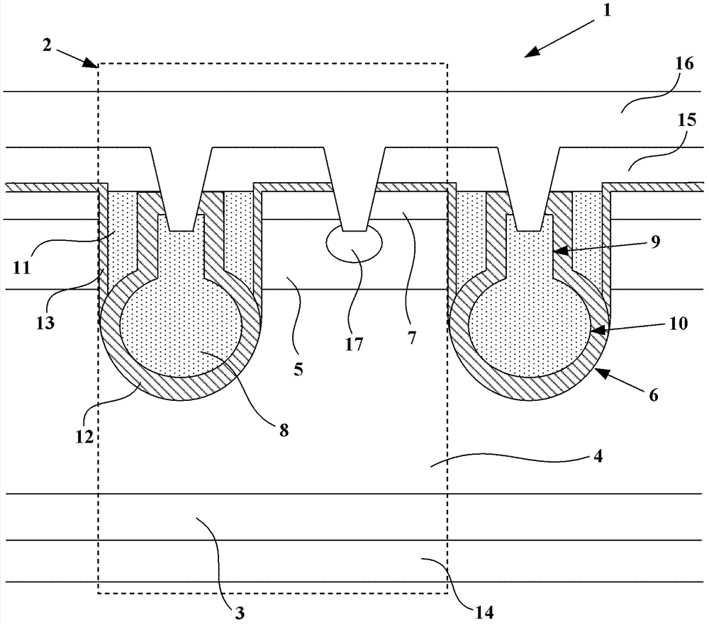
[0056] Embodiment: a trench MOS device with low gate-to-drain capacitance, the active region 1 of the device is composed of several trench MOS unit cells 2 arranged in parallel; on the lateral section of the active region 1, each trench The MOS unit cell 2 includes a heavily doped drain region 3 of the first conductivity type located on the back side of the silicon wafer, an epitaxial layer 4 of the first conductivity type lightly doped above the drain region 3; The well layer 5 of the second conductivity type in the inner upper part; the trench 6 passing through the well layer 5 and extending to the epitaxial layer 4; the first conductive type in the upper part of the well layer 5 and located around the trench 6 type heavily doped first source region 7;

[0057] The bottom of the groove 6 is semi-circular arc-shaped, and the diameter of this semi-circular arc is not smaller than the opening size of the groove 6. The second electrode region is located in the center of the groo...


PUM


Abstract

The invention discloses a low grid-drain capacitance grooved metal oxide silicon (MOS) device and a manufacturing method thereof. The low grid-drain capacitance grooved MOS device comprises a plurality of grooved MOS unit cells which are arranged in parallel; each unit cell comprises a groove and a lug boss structure which is formed by a monocrystalline silicon extension layer; the bottom part of each groove is in a semicircular shape, the center of each groove is provided with a second source area which is used as a source area and is filled by conductive polysilicon, and the second source area consists of a rectangular block and an elliptic block which is arranged on the lower end of the rectangular block; a first conductive-type heavily-doped polysilicon grid which is used as a grid area is arranged on the periphery of each rectangular block and in each groove, the upper surface of the polysilicon grid is ended on the upper surface of the extension layer, the lower surface of the polysilicon grid is a curved surface, and the deepest place of the curved surface of the polysilicon grid is free from exceeding a transverse middle line of each elliptic block; and a silicon dioxide layer is respectively arranged between each polysilicon grid and each second source area and between the extension layer lug boss structures. Due to the adoption of the low grid-drain capacitance grooved MOS device, the grid-drain parasitic capacitance can be effectively reduced so as to effectively reduce the switching loss when the device is in work, and at the same time the capacity for inhibiting the mistake starting when the device stays at a switching work state can be remarkably enhanced.

Description

technical field [0001] The invention relates to a power MOS field effect transistor device and a manufacturing method thereof, in particular to a trench MOS field effect transistor device with low gate-drain capacitance and a manufacturing method thereof. Background technique [0002] Trench MOS devices are widely used in power circuits as switching devices to connect power and loads. With the improvement of power efficiency requirements and equipment miniaturization requirements, trench MOS devices need to work at higher switching frequencies, and the resulting high switching losses of devices become unacceptable. The main cause of switching loss is the parasitic capacitance Cgd between the gate and drain of the MOS device. During the switching operation of the MOS device, due to the existence of the parasitic capacitance Cgd, the phase between the current signal flowing through the source and drain and the source-drain voltage signal is generated. Poor, causing power loss...

Claims


Application Information

Patent Timeline
Patent Type & Authority Patents(China)
IPC IPC(8): H01L29/78H01L29/06H01L29/423H01L21/336
Inventor 刘伟王凡
Owner SUZHOU SILIKRON SEMICON CO LTD
Learn More