
Scanning test method

A scanning test and memory technology, applied in the direction of digital circuit testing, electronic circuit testing, etc., can solve the problems of increasing the scanning test cost and high memory, and achieve the effect of reducing the scanning test cost, low storage depth and cost.

Active Publication Date: 2012-05-02
SHANGHAI HUAHONG GRACE SEMICON MFG CORP
View PDF12 Cites 0 Cited by
  • Summary
  • Abstract
  • Description
  • Claims
  • Application Information

AI Technical Summary

Problems solved by technology

This has high memory requirements, which increases the cost of scan testing

Method used


Image

  • Scanning test method
  • Scanning test method

Examples


Embodiment Construction

[0021] In order to make the above objects, features and advantages of the present invention more comprehensible, specific implementations of the present invention will be described in detail below in conjunction with the accompanying drawings.

[0022] In the following description, many specific details are set forth in order to fully understand the present invention, but the present invention can also be implemented in other ways than those described here, so the present invention is not limited by the specific embodiments disclosed below.

[0023] In the prior art, the price of the memory testing machine is relatively low. However, the test pattern used when testing the memory is a regularly changing test pattern, and at least two larger DRAM memories are used to store codes or to collect failure information of the memory under test, which is different from logic integrated circuit testing. The patterns are different (corresponding to tens of millions of electronic component...


PUM


Abstract

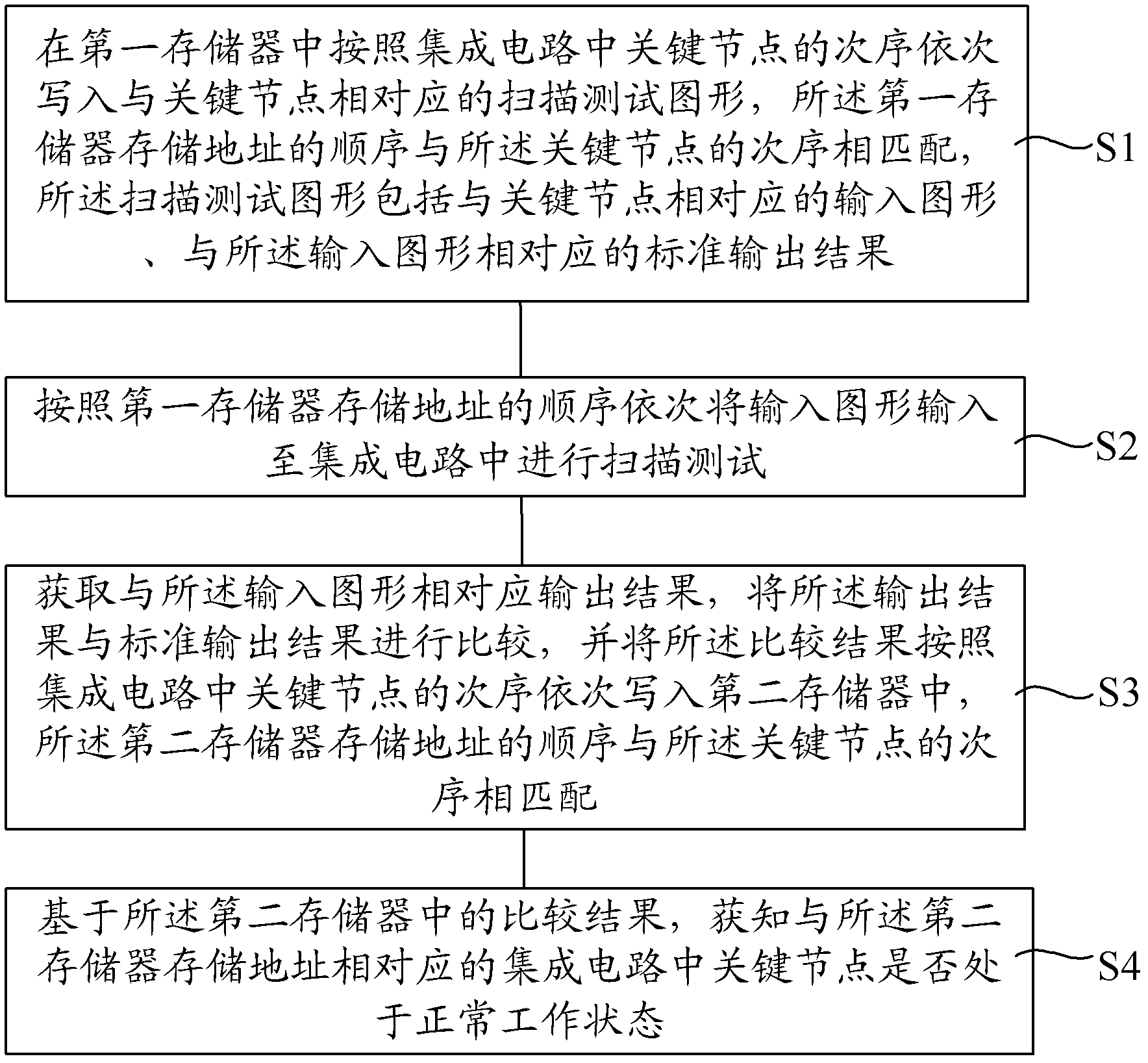
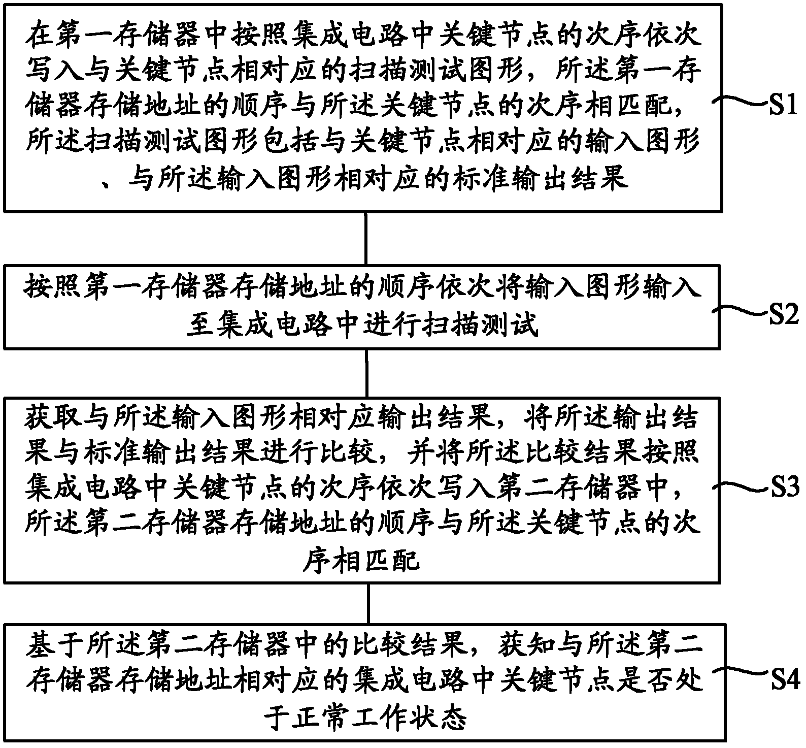
A scanning test method comprises the following steps: successively writing a scanning test graph corresponding to key nodes in a first memory according to an sequence of the key nodes in an integrated circuit (IC), wherein the sequence of a first memory storage address is matched with the sequence of the key nodes, and the scanning test graph comprises: an input graphs corresponding to the key nodes and a standard output result corresponding to the input graphs; inputting the input graphs successively into the IC according to the sequence of the first memory storage address and performing scanning test; acquiring an output result corresponding to the input graphs, comparing the output result with a standard output result and successively writing a comparison result in a second memory according to the sequence of the key nodes, wherein the sequence of a second memory storage address is matched with the sequence of key nodes; based on the comparison result in the second memory, knowing whether the key nodes corresponding to the second memory storage address in the IC are in a normal working state. By using the method of the invention, scanning test costs can be reduced.

Description

technical field [0001] The invention relates to the field of integrated circuit testing, in particular to a method for scanning and testing integrated circuits. Background technique [0002] With the development of electronic products in the direction of miniaturization, large-scale integrated circuits (LSI) in consumer electronics fields such as laptop computers, CPU circuits, micro mobile communication circuits (mobile phones, etc.), digital audio and video circuits, communication machines, digital cameras, etc. , IC) and VLSI (Very LargeScale Integration, VLSI), require the shape of the semiconductor chip to be made smaller and thinner. [0003] In the integrated circuit manufacturing process, it is necessary to test the formed integrated circuit to ensure that it can basically meet the characteristics of the device or design specifications. Specifically, the test usually includes verification of voltage, current, timing and function. If the test results do not meet the ...

Claims


Application Information

Patent Timeline
Patent Type & Authority Applications(China)
IPC IPC(8): G01R31/317
Inventor 索鑫
Owner SHANGHAI HUAHONG GRACE SEMICON MFG CORP
Learn More