Silicon wafer and production method thereof

A technology of silicon wafers and silicon single crystals, applied in chemical instruments and methods, semiconductor/solid-state device manufacturing, crystal growth, etc., can solve problems such as increasing wafer production costs

Inactive Publication Date: 2012-03-14
SILTRONIC AG
View PDF8 Cites 6 Cited by
  • Summary
  • Abstract
  • Description
  • Claims
  • Application Information

AI Technical Summary

Problems solved by technology

[0029] Therefore, the production cost of the wafer is increased

Method used


Image

  • Silicon wafer and production method thereof
  • Silicon wafer and production method thereof
  • Silicon wafer and production method thereof

Examples


Embodiment 1

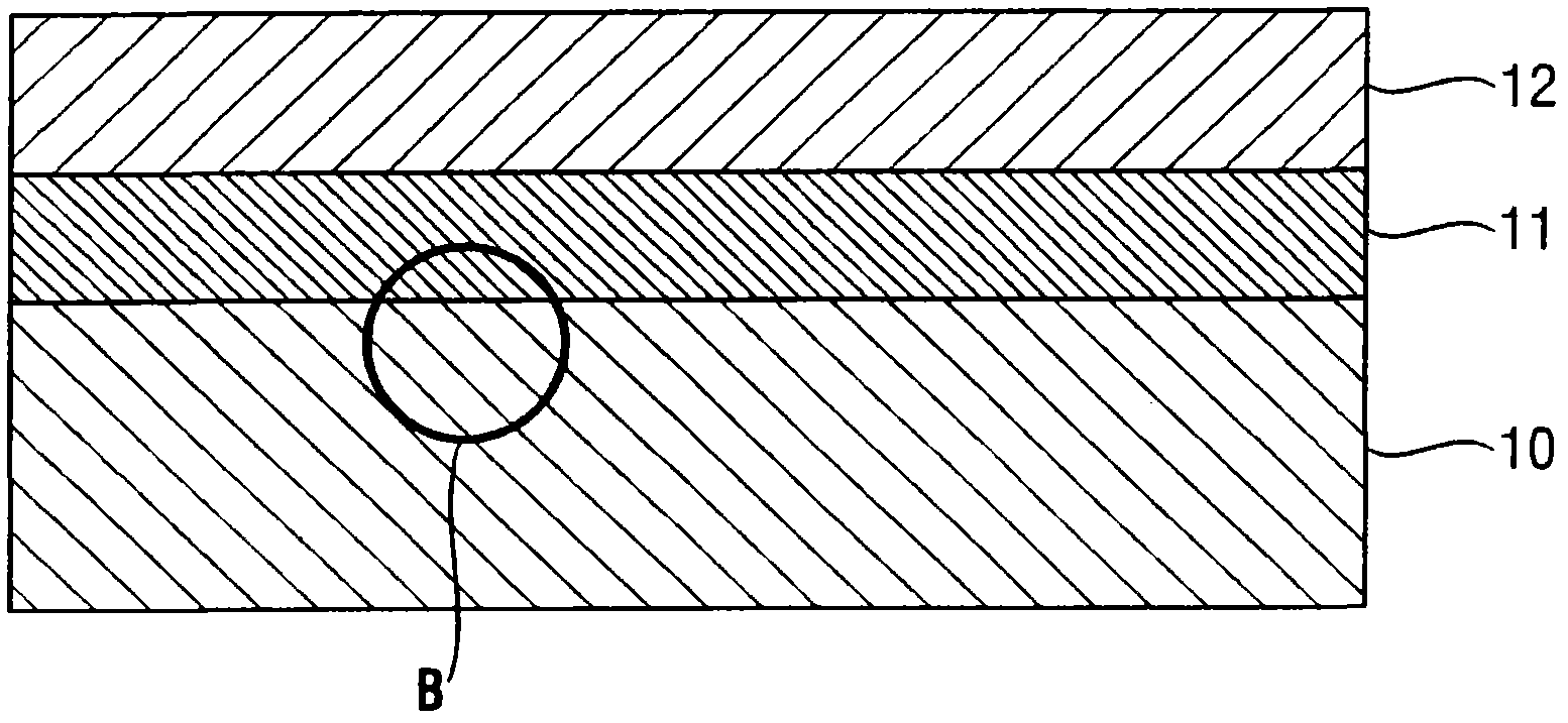
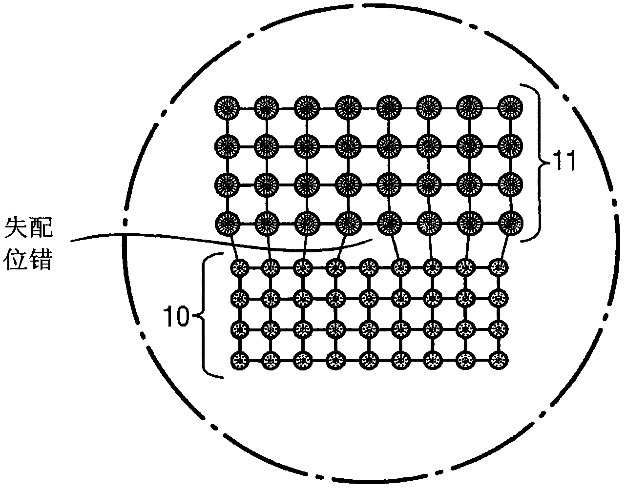
[0170] The mirror wafers were grown by the dicing Czochralski method with a diameter of 200 mm and a phosphorus concentration of 5 × 10 14 atoms / cm 3 n-type silicon single crystal ingots and manufactured by performing a wafer production process on sliced ​​wafers.

[0171] Then, the wafer was set in a separate loading type apparatus for epitaxial vapor phase growth in a lamp heating method, and heat treatment was performed in a hydrogen atmosphere at 1100° C. for cleaning.

[0172] Then, supply SiHCl at 1050°C and standard pressure 3 、GeCl 4 and PH 3 mixed reaction gas. By CVD method, the thickness of 10 μm is grown on the wafer, and the donor concentration (phosphorus concentration) is 7×10 19 atoms / cm 3 And the material (germanium concentration) to adjust the lattice constant is 9×10 19 atoms / cm 3 of the first epitaxial layer.

[0173] The germanium concentration and phosphorus concentration of the first epitaxial layer were measured by SIMS (Secondary Ion Mass Spec...

Embodiment 2

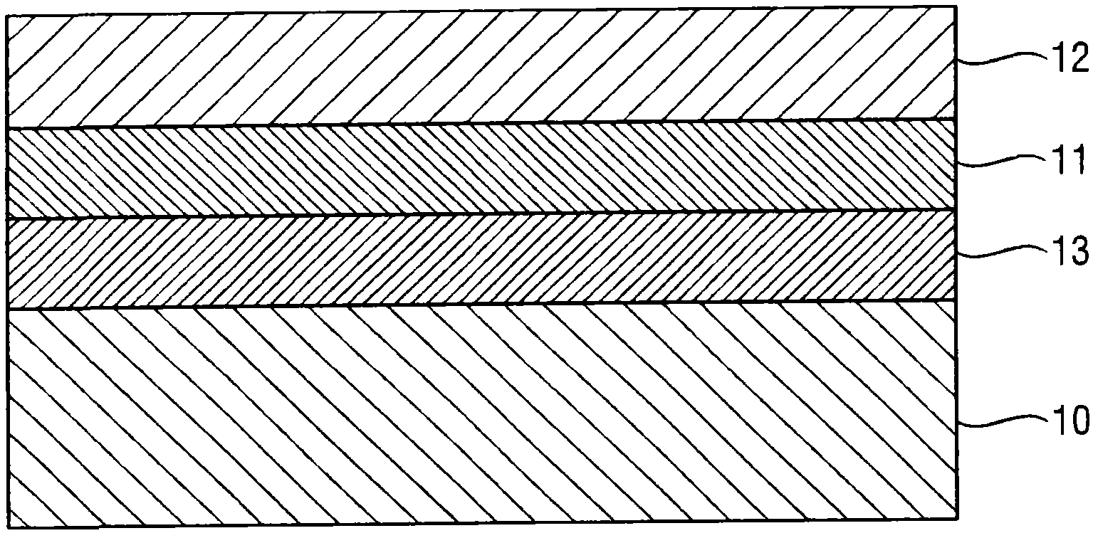
[0179] The mirror wafers were grown by the dicing Czochralski method with a diameter of 200 mm and a phosphorus concentration of 5 × 10 14 atoms / cm 3 n-type silicon single crystal ingots and manufactured by performing a wafer production process on sliced ​​wafers.

[0180] Then, the wafer was set in a separate loading type apparatus for epitaxial vapor phase growth in a lamp heating method, and heat treatment was performed in a hydrogen atmosphere at 1100°C.

[0181] Then, supply SiHCl at 1050°C and standard pressure 3 、GeCl 4 and B 2 h 6 mixed reaction gas. Grown on the wafer by CVD with a thickness of 10 μm and a receptor concentration (boron concentration) of 5×10 19 atoms / cm 3 And the material (germanium concentration) to adjust the lattice constant is 3.3×10 20 atoms / cm 3 The third epitaxial layer (p-type).

[0182] In order to control the concentration of germanium and boron in the third epitaxial layer, B can be changed 2 h 6 gas or GeCl 4 The concentration...


PUM


Abstract

To provide a silicon wafer comprising: a silicon substrate; a first epitaxial layer laid on one side of the silicon wafer, wherein the absolute value of the difference between the donor concentration and the acceptor concentration is set to equal or more than 110 18 atoms / cm 3 ; and a second epitaxial layer laid on the first epitaxial layer, whose conductivity type is the same as for said first epitaxial layer, wherein the absolute value of the difference between the donor concentration and the acceptor concentration is set to equal or less than 510 17 atoms / cm 3 ; wherein, by doping a lattice constant adjusting material into the first epitaxial layer, the variation amount ((a 1 - a Si ) / a Si ) of the lattice constant of the first epitaxial layer (a 1 ) relative to the lattice constant of the silicon single crystal (a Si ) as well as the variation amount ((a 2 - a Si ) / a Si ) of the lattice constant of the second epitaxial layer (a 2 ) relative to the lattice constant of the silicon single crystal (a si ) are controlled less than the critical lattice mismatches.

Description

technical field [0001] The present invention relates to the technical field of silicon wafers for semiconductor devices. Specifically, the present invention relates to a technique for suppressing misfit dislocations generated in a silicon wafer incorporating an epitaxially grown thin film. Background technique [0002] Currently, silicon wafers used for semiconductor devices require defect-free regions and high gettering capabilities in device active regions on their surface layers. [0003] As an example of meeting these requirements, epitaxial wafers using highly doped substrates are generally known. [0004] An example of such a wafer includes a p / p+ substrate. The p / p+ substrate is fabricated by making a boron concentration of about 5×10 19 atoms / cm 3 The p+ substrate, the p+ substrate is mirror-polished and cleaned; then a device active layer with a thickness of 5 μm is epitaxially grown on the mirror-polished p+ substrate by vapor phase epitaxy, wherein the device ...

Claims


Application Information

Patent Timeline
Patent Type & Authority Applications(China)
IPC IPC(8): H01L29/00H01L29/36
CPCH01L21/02381H01L21/0245H01L21/02532H01L21/02576H01L21/0262C30B29/06H01L21/20
Inventor 出合博之高山诚治
Owner SILTRONIC AG
Why Eureka
Try Eureka