Unpolarized tunable guided-mode resonance filter system and method for measuring nanometer gap
A nano-gap and optical filter technology, which is applied to optical filters, measuring devices, optical devices, etc., can solve the problems of inability to detect nano-gap changes, measurement accuracy intensity changes, etc., and achieves simple structure, simplified requirements, easy to use build effect
- Summary
- Abstract
- Description
- Claims
- Application Information
AI Technical Summary
Problems solved by technology
Method used
Image

Examples
Embodiment 1
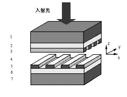
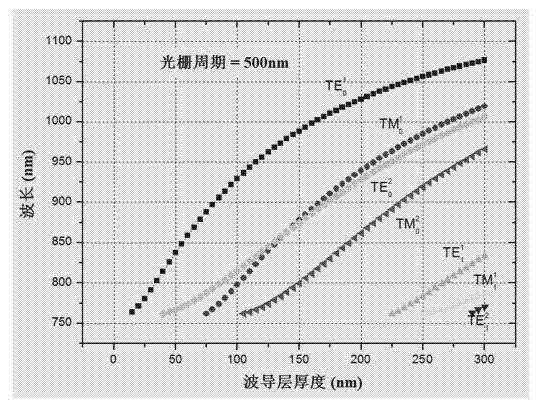
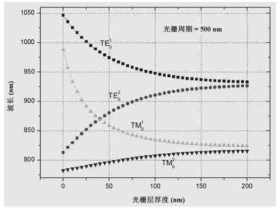
[0062] On the basis of the foregoing embodiments, the waveguide layer material is selected as titanium dioxide (TiO2) with a refractive index of 2.35, the grating layer material is silicon dioxide (SiO2) with a refractive index of 1.46, the grating period is 500 nm, and the grating fill factor is f = 0.5, the thickness of the grating layer is 40nm, the thickness of the air gap is zero, change the thickness of the two waveguide layers, and calculate the relationship between the resulting resonance peak wavelength position and the thickness of the waveguide layer, see the attached figure 2 shown. Then the thickness of the waveguide layer is selected as 145nm, the thickness of the two grating layers is changed, and the relationship between the resulting resonance peak wavelength position and the thickness of the grating layer is calculated, see the attached image 3 shown. Then select the thickness of the grating layer to be 40nm, change the thickness of the air gap, and calcul...
Embodiment 2
[0069] On the basis of the above embodiments, the material of the waveguide layer is zinc sulfide (ZnS) with a refractive index of 2.45, and the material of the grating layer is magnesium fluoride (MgF2) with a refractive index of 1.38. 2 ), the grating period is 1000nm, the grating fill factor is f = 0.5, the thickness of the grating layer is 80nm, and the thickness of the air gap is zero. Change the thickness of the two waveguide layers, and calculate the resulting relationship between the wavelength position of the resonance peak and the thickness of the waveguide layer relationship, see attached Figure 5 shown. Then, the thickness of the waveguide layer is selected as 200nm, the thickness of the two grating layers is changed, and the relationship between the resulting resonance peak wavelength position and the thickness of the grating layer is calculated, see the attached Image 6 shown. Then select the thickness of the grating layer to be 80nm, change the thickness of ...
Embodiment 3
[0072] On the basis of the above embodiments, the material of the waveguide layer is selected as zirconia (ZrO2) with a refractive index of 2.2. 2 ), the grating layer material is calcium fluoride (CaF 2 ), the grating period is 330nm, the grating fill factor is f = 0.5, the thickness of the grating layer is 26.4nm, and the thickness of the air gap is zero. Change the thickness of the two waveguide layers, and calculate the resulting resonance peak wavelength position and waveguide layer thickness relationship between, see attached Figure 8 shown. Then the thickness of the waveguide layer is selected as 119nm, the thickness of the two grating layers is changed, and the relationship between the wavelength position of the resonant peak and the thickness of the grating layer is calculated, see the attached Figure 9 shown. Then select the thickness of the grating layer to be 26.4nm, change the thickness of the air gap, and calculate the relationship between the resulting wave...
PUM
 Abstract
Description
Claims
Application Information
 - R&D
- Intellectual Property
- Life Sciences
- Materials
- Tech Scout
- Unparalleled Data Quality
- Higher Quality Content
- 60% Fewer Hallucinations
Browse by: Latest US Patents, China's latest patents, Technical Efficacy Thesaurus, Application Domain, Technology Topic, Popular Technical Reports.
© 2025 PatSnap. All rights reserved.Legal|Privacy policy|Modern Slavery Act Transparency Statement|Sitemap|About US| Contact US: help@patsnap.com