Manufacturing method of silicon epitaxial wafer for MMW (millimeter wave) avalanche diode

A technology for silicon epitaxial wafers and manufacturing methods, which are applied in the directions of final product manufacturing, chemical instruments and methods, sustainable manufacturing/processing, etc., to achieve the effects of stable epitaxial layer thickness, low growth temperature, and reduced compensation degree

Active Publication Date: 2014-03-19
NANJING GUOSHENG ELECTRONICS
View PDF2 Cites 0 Cited by
  • Summary
  • Abstract
  • Description
  • Claims
  • Application Information

AI Technical Summary

Problems solved by technology

The influence of variable flow growth method and conventional epitaxial growth on the distribution of N-type impurities at the PN interface such asFigure 3, the distribution of the conventional growth method is flat, and the distribution of the variable flow growth method is steep

Method used


Image

  • Manufacturing method of silicon epitaxial wafer for MMW (millimeter wave) avalanche diode
  • Manufacturing method of silicon epitaxial wafer for MMW (millimeter wave) avalanche diode
  • Manufacturing method of silicon epitaxial wafer for MMW (millimeter wave) avalanche diode

Examples


Embodiment Construction

[0030] Below in conjunction with accompanying drawing and specific embodiment the present invention is described in detail:

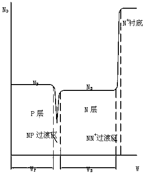
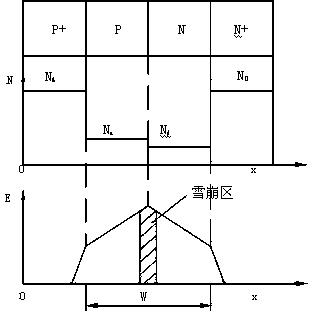
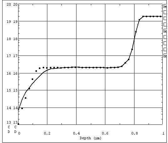
[0031] The size of the transition region directly affects the output power and conversion efficiency of the avalanche diode, the concentration of the P-type and N-type epitaxial layers directly affects the operating frequency of the avalanche diode, and the thickness of the P-type and N-type epitaxial layer directly affects the breakdown voltage of the avalanche diode. The invention has been created. The invention is a multi-layer epitaxy technology developed based on the theory of self-doping generation mechanism, suppression method and solid-state diffusion. The special requirements put forward for avalanche diodes, compared with conventional epitaxy, its technology is characterized by controlling the gas corrosion amount of HCl and encapsulating the substrate surface with a pure epitaxial layer; using lower growth temperature and lower deposition ra...


PUM

PropertyMeasurementUnit
thicknessaaaaaaaaaa
thicknessaaaaaaaaaa

Abstract

The invention relates to a silicon epitaxial wafer, and in particular relates to a manufacturing method of a silicon epitaxial wafer for an MMW (millimeter wave) avalanche diode. The manufacturing method is characterized by comprising the following steps of: firstly, adopting HCl (hydrogen chloride) to corrode impurities and metal atoms on a substrate surface and using high-flow hydrogen to blow the impurities and the metal atoms down; secondarily, growing a first epitaxial layer on the high-concentration substrate surface and packing the surface and edges of a substrate slice; growing a second N-type epitaxial layer; and finally, growing a third P-type epitaxial layer. The manufacturing method has the beneficial effects that a clean growth region can be formed; N-type and P-type doping agents are added before the N-type and P-type epitaxial layers are grown, thus the stable thicknesses of the epitaxial layers can be obtained; and a transition region can be reduced by adopting lower growth temperature and deposition rate.

Description

technical field [0001] The invention relates to a silicon epitaxial wafer, in particular to a method for manufacturing a silicon epitaxial wafer for a millimeter-wave avalanche diode, and belongs to the field of silicon epitaxial wafer manufacturing. Background technique [0002] In the millimeter-wave band, avalanche diodes have good application prospects due to their large output power and high conversion efficiency, and are one of the solid-state power devices that have received widespread attention. Its symmetrical and uniformly doped double-drift (DDR) structure (P + PNN + ) with a single-drift structure (P + NN + ) Compared with it, it has the characteristics of large area and small thermal resistance, which improves the output power and conversion efficiency of the device. To obtain the maximum output power and efficiency of the device in the required frequency band, the first is to optimize the internal structure of the device, and the internal structure of the ...

Claims


Application Information

Patent Timeline
Patent Type & Authority Patents(China)
IPC IPC(8): H01L31/18C30B29/06
CPCY02P70/50
Inventor 马林宝马利行金龙
Owner NANJING GUOSHENG ELECTRONICS
Why Eureka
Try Eureka