Band gap reference voltage source circuit

A reference voltage source, DC voltage source technology, applied in the direction of regulating electrical variables, control/regulating systems, instruments, etc., can solve the problem of poor linear adjustment rate without op-amp, increase circuit complexity and power consumption, stability and linearity Problems such as poor adjustment rate, to achieve the effect of small circuit chip area, improved linear adjustment rate, and high stability

Inactive Publication Date: 2012-01-25
JINAN UNIVERSITY
View PDF4 Cites 9 Cited by
  • Summary
  • Abstract
  • Description
  • Claims
  • Application Information

AI Technical Summary

Problems solved by technology

[0008] However, the minimum supply voltage min[V DD ] subject to V EB +V T +2V Dsat limit, here V Dsat is the overdrive voltage of the MOS tube
Since V T >0.5V, V Dsat >0.1V,V EB ≥0.7V, so min[V DD ]>1.4V, and the drain voltage of each MOS tube is different, so the linear adjustment rate of the circuit without op amp is poor
[0009] To sum up, the current bandgap reference voltage source circuits with operational amplifiers use operational amplifiers to stabilize the output voltage. Since they are not directly used to generate output voltages, the complexity and power consumption of these circuits are increased; The bandgap reference voltage source circuit has poor stability and linear regulation due to the limited minimum supply voltage

Method used


Image

  • Band gap reference voltage source circuit
  • Band gap reference voltage source circuit
  • Band gap reference voltage source circuit

Examples


Embodiment

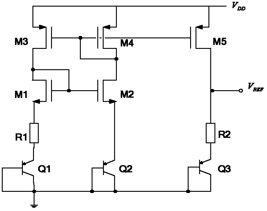
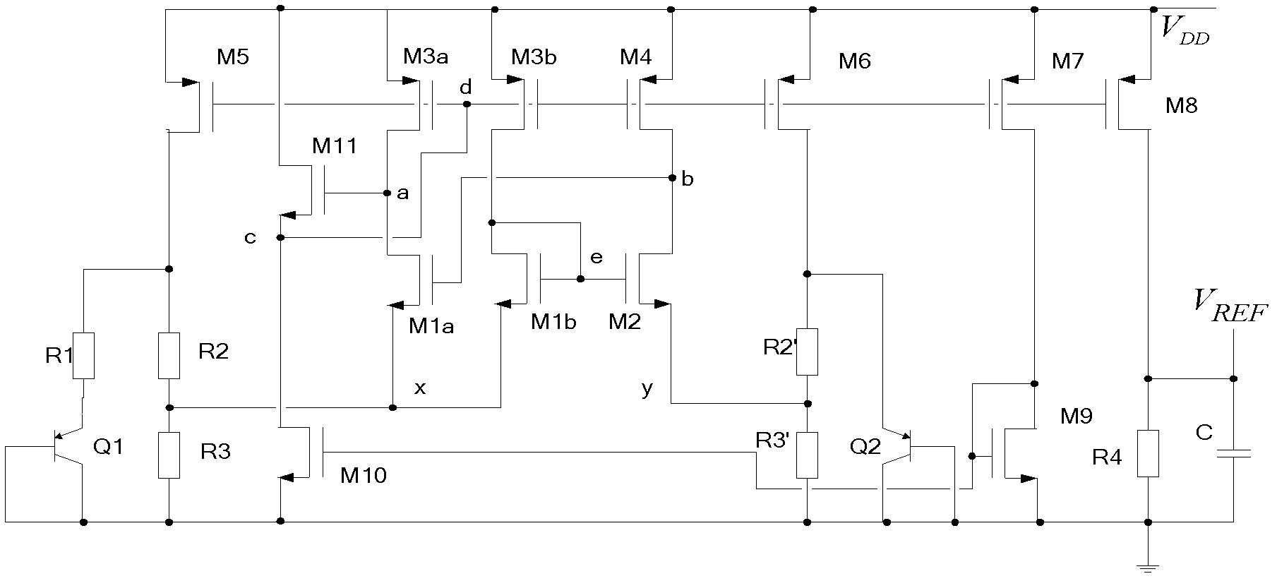
[0023] figure 2 The bandgap reference voltage source circuit designed by the present invention by adopting methods such as improving the feedback loop and adjusting the resistance value is given. like figure 2 As shown, the present invention uses MOS tube M1a, MOS tube M1b, MOS tube M2, MOS tube M3a, MOS tube M3b, MOS tube M4, MOS tube M5 and MOS tube M6 to form a feedback loop, instead of figure 1 The feedback loop MOS transistors M1-M4 of the traditional bandgap reference voltage source circuit are shown, and the resistance structure in the traditional bandgap reference voltage source circuit is adjusted.

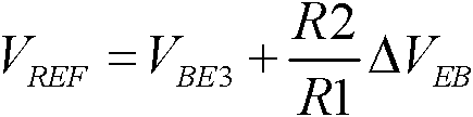
[0024] from figure 2 It can be seen that the present invention includes a feedback loop composed of MOS transistors, a first set of adjustment resistors connected in series at the feedback end of the feedback loop, and a second set of adjustment resistors connected in series at the output end of the feedback loop. The first group of adjusting resistors includes resi...


PUM


Abstract

The invention discloses a band gap reference voltage source circuit, which comprises a regulating resistor and a feedback loop consisting of MOS (Metal Oxide Semiconductor) tubes, and is characterized in that: the regulating resistor comprises a first group of regulating resistors which is connected in series to the feedback end of the feedback loop and a second group of regulating resistors which is connected in series to the output end of the feedback loop; the first group of regulating resistors comprises a resistor R2 and a resistor R3 which are connected in series; the second group of regulating resistors comprises a resistor R2' and a resistor R3' which are connected in series; the resistance value of the first group of regulating resistors is equal to that of the second group of regulating resistors; the resistance value of the resistor R2 is equal to that of the resistor R2'; the resistance value of the resistor R3 is equal to that of the resistor R3'; and the resistance values of the R2, R2', R3 and R3' are adjustable. The linear regulating rate of the circuit is remarkably higher than that of the conventional operational amplifier-free band gap reference voltage source circuit, so that the stability of the circuit is higher.

Description

technical field [0001] The invention relates to a bandgap reference voltage source circuit, in particular to a bandgap reference voltage source circuit suitable for white light LED drive chips and power management chips. Background technique [0002] The bandgap reference voltage source suitable for white LED driver chips and power management chips can provide accurate, stable, and temperature-independent reference voltages. Its working principle is to provide emitter bias voltage V by bipolar transistors. BE , and by the ΔV between the two transistors BE Generate thermal voltage V T And amplified by α times through the resistor network, the two voltages are superimposed V REF =V BE +αV T Finally, by choosing an appropriate magnification α, the temperature drift of the two voltages can be offset against each other, thereby obtaining a reference voltage with a temperature coefficient of zero at a certain temperature. [0003] At present, the mainstream bandgap reference ...

Claims


Application Information

Patent Timeline
Patent Type & Authority Applications(China)
IPC IPC(8): G05F3/30
Inventor 邓婉玲黄君凯杨帆
Owner JINAN UNIVERSITY
Why Eureka
Try Eureka