
Method for manufacturing electronic device and separation apparatus used therefor

A technology of electronic devices and manufacturing methods, applied in semiconductor/solid-state device manufacturing, electrical solid-state device, printed circuit manufacturing, etc.

Inactive Publication Date: 2011-08-31
ASAHI GLASS CO LTD
View PDF10 Cites 48 Cited by
  • Summary
  • Abstract
  • Description
  • Claims
  • Application Information

AI Technical Summary

Problems solved by technology

[0028] In addition, the peeling device described in Patent Document 8 is a device for peeling a glass substrate, etc. held by adsorption on a suction sheet, from the suction sheet. Peeling without leaving the resin layer on the thin glass substrate

Method used


Image

  • Method for manufacturing electronic device and separation apparatus used therefor
  • Method for manufacturing electronic device and separation apparatus used therefor
  • Method for manufacturing electronic device and separation apparatus used therefor

Examples


Embodiment 1

[0438] Examples of the present invention will be described.

[0439] First of all, for the vertical 720mm, horizontal 600mm, plate thickness 0.4mm, linear expansion coefficient 38×10 -7 A support glass substrate (manufactured by Asahi Glass Co., Ltd., AN100, non-alkali glass substrate) at / °C was cleaned by washing with pure water and UV.

[0440] Next, on the supporting glass substrate, the size of 705 mm in length and 595 mm in width is applied by a screen printing machine (coating amount: 30 g / m 2 ) Silicone for solvent-free addition reaction type release paper (Shin-Etsu Silicone Co., Ltd., KNS-320A, viscosity: 0.40 Pa·s, 100 parts by mass, platinum-based catalyst (Shin-Etsu Silicone Co., Ltd., CAT-PL-56) 2 parts by mass of the mixture.

[0441] Next, this was heated and cured at 180° C. in the air for 30 minutes to obtain a silicone resin layer with a thickness of 20 μm on the surface of the supporting glass substrate.

[0442] Secondly, for the vertical 715mm, horizon...

Embodiment 2

[0474] In Example 2, except having changed the board|substrate into the polyethylene terephthalate resin board|substrate of thickness 0.1mm, it carried out similarly to Example 1, produced the laminated body B, and performed the same test as peeling test 3. As a result, the support body and the polyethylene terephthalate resin substrate can be peeled off without damaging the laminated body B. The charged voltage of the polyethylene terephthalate resin substrate after peeling was +0.3 kV.

Embodiment 3

[0476] In Example 3, the laminate C was produced in the same manner as in Example 1 except that the substrate was changed to a mirror-finished stainless steel (SUS304) substrate with a thickness of 0.1 mm, and the same test as in the peeling test 3 was performed. As a result, the support body and the stainless steel substrate can be peeled off without damaging the laminate C. The charged voltage of the stainless steel substrate after peeling was +0.02 kV.


PUM

PropertyMeasurementUnit
Plate thicknessaaaaaaaaaa
Linear expansion coefficientaaaaaaaaaa
Thicknessaaaaaaaaaa

Abstract

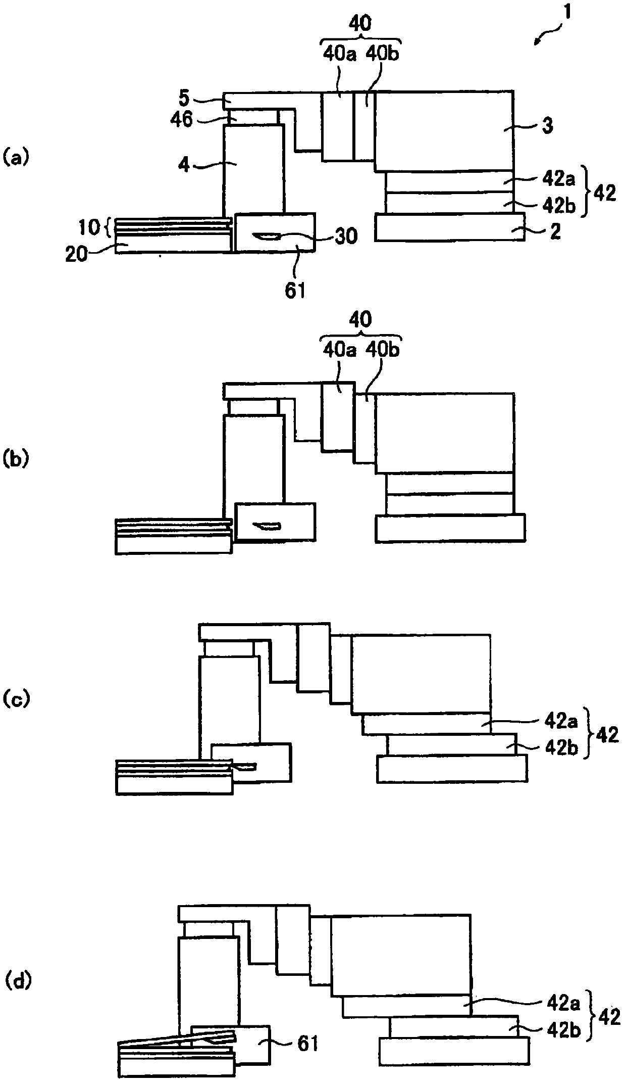
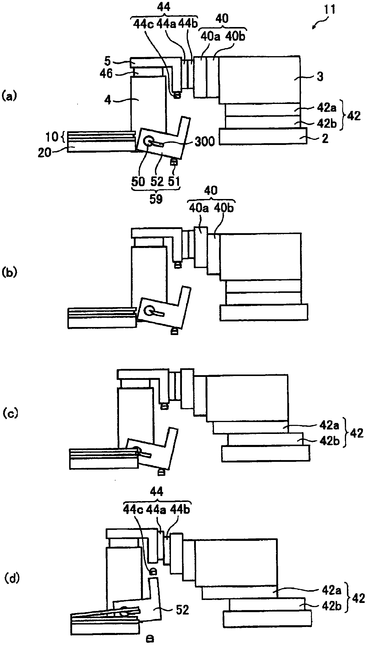
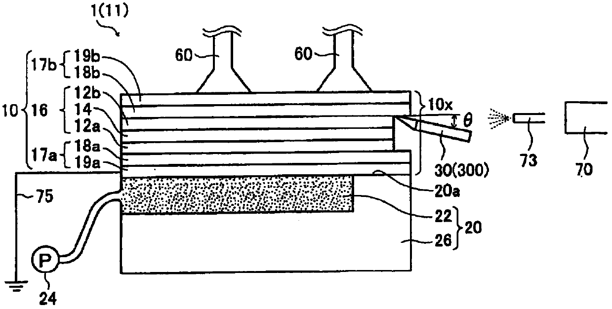
Provided are a method for manufacturing an electronic device and a separation apparatus used therefore, wherein a substrate and a resin layer closely connected thereto can be easily separated and removed within a short space of time without damage. When a support (17b) comprised of a support substrate (19b) and a resin layer (18b) is separated from a support-provided electronic device (10) which has a substrate (12b) having an electronic device member (14) and a resin layer (18b) which is secured to a support substrate (19b) and which is closely connected to the substrate (12b), a main surface on which a substrate (17b) to be separated later is not mounted is closely connected to a securing surface (20a) of a stage (20) to secure the support-provided electronic device (10), and a knife (30) is inserted between interfaces of the resin layer (18b) and the substrate (12b) of the support (17b) to be separated, at an end surface of the support-provided electronic device (10) secured to the stage (20) to thereby separate the support (17b) and an electronic device (16), thus to solve the aforementioned problem.

Description

technical field [0001] The present invention relates to a manufacturing method of an electronic device and a peeling device used in the method. Background technique [0002] In recent years, liquid crystal display devices (LCD) and organic EL display devices (OLED) have been widely used as display devices. In particular, in the field of portable display devices such as mobile phones and mobile phones, reduction in weight and thickness of display devices is required. [0003] Similarly, electronic devices such as solar cells, thin-film secondary batteries, and semiconductor wafers with circuits formed on their surfaces are also seeking to reduce their weight and thickness. [0004] In response to this, substrates such as glass, resin, and metal used in electronic devices such as display devices are becoming thinner. [0005] In the case of a glass substrate, as a method of reducing the plate thickness, the following method is generally carried out, before or after forming t...

Claims


Application Information

Patent Timeline
IPC IPC(8): G09F9/00G02F1/1333G09F9/30
CPCH01L51/56H05K3/007H01L51/003B65H2301/51122G02F1/1303H01L21/67092H10K71/80H10K71/40H10K71/70G02F1/1333G02F1/13
Inventor 江畑研一近藤聪伊藤泰则
Owner ASAHI GLASS CO LTD
Learn More