Method for forming one time programmable (OTP) device

A device and patterning technology, which is applied in semiconductor/solid-state device manufacturing, electrical components, circuits, etc., can solve the problems of dielectric layer etching, device data retention ability reduction, thickness reduction, etc.

Active Publication Date: 2015-02-25
SHANGHAI HUAHONG GRACE SEMICON MFG CORP
View PDF3 Cites 0 Cited by
  • Summary
  • Abstract
  • Description
  • Claims
  • Application Information

AI Technical Summary

Problems solved by technology

[0008] The problem solved by the invention is that the dielectric layer above the floating gate is etched and its thickness becomes smaller during the formation of the OTP device, resulting in a decrease in the data retention capability of the device

Method used


Image

  • Method for forming one time programmable (OTP) device
  • Method for forming one time programmable (OTP) device
  • Method for forming one time programmable (OTP) device

Examples


Embodiment Construction

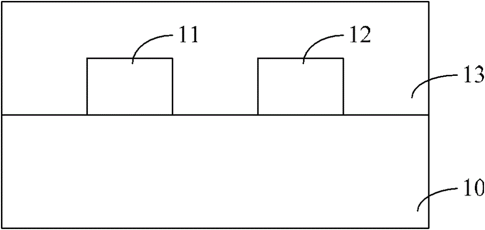
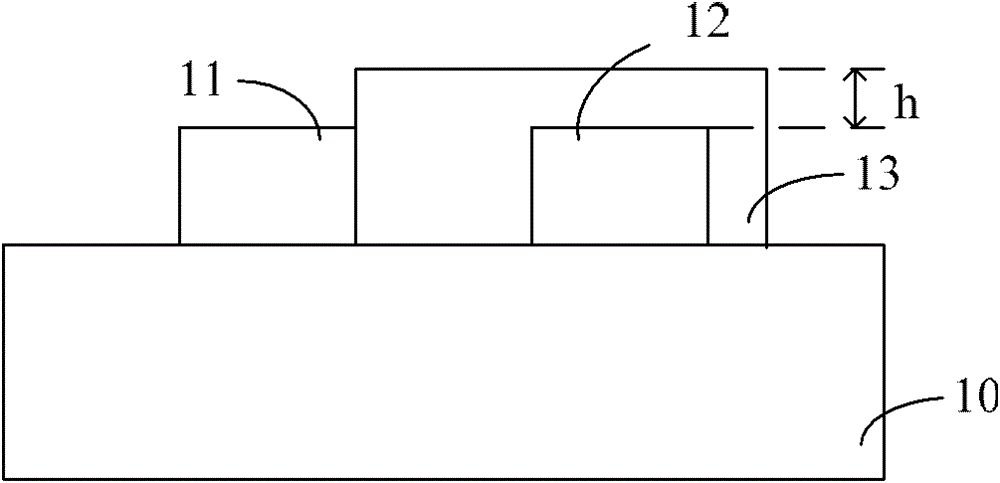
[0030] In the prior art, when the remaining dielectric layer on the surface of the semiconductor substrate is etched away, the dielectric layer above the floating gate is also etched, resulting in the thickness of the dielectric layer above the floating gate being too small, which affects the data retention capability of the OTP device.

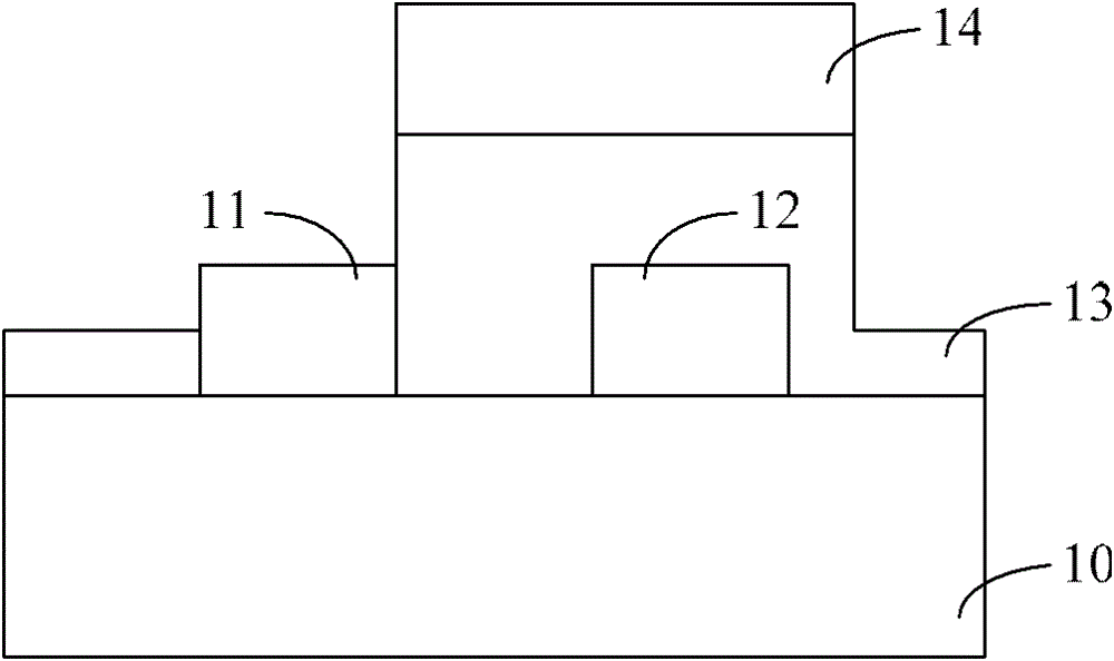
[0031] In this technical solution, an anti-reflection layer and a photoresist layer are sequentially formed on the dielectric layer, and the photoresist layer is patterned to define the pattern of the floating gate; then the patterned photoresist layer is used as a mask film, etch the anti-reflection layer and dielectric layer until the surface of the selection gate is exposed; after removing the patterned photoresist, use the anti-reflection layer as a mask to etch and remove all The remaining dielectric layer on the surface of the semiconductor substrate. Since the anti-reflection layer is used as a mask to etch and remove the remaining die...


PUM


Abstract

The invention discloses a method for forming a one time programmable (OTP) device. The method comprises the following steps of: providing a semiconductor substrate, wherein a selective gate and a floating gate are formed on the semiconductor substrate side by side, a dielectric layer is also formed on the semiconductor substrate to cover the surface of the semiconductor substrate, the selective gate and the floating gate; forming an antireflection layer and a photoresist layer on the surface of the dielectric layer in turn, patterning the photoresist layer and defining a pattern of the floating gate; etching the antireflection layer and the dielectric layer by taking the patterned photoresist layer as a mask until the surface of the selective gate is exposed; removing the patterned photoresist layer; and etching to remove the remaining dielectric layer on the surface of the semiconductor substrate by taking the antireflection layer as the mask. By the method, the problem of over-small thickness due to the etching of the dielectric layer above the floating gate can be solved; and the method contributes to preventing the data retention capacity of the OTP device from being affected.

Description

technical field [0001] The invention relates to the technical field of semiconductors, in particular to a method for forming an OTP device. Background technique [0002] One Time Programmable (OTP, One Time Programmable) device is a commonly used memory, which belongs to read-only memory. It is named because it can only be programmed once. When the OTP device leaves the factory, the general storage content is 0 or 1. Users can program it according to their own needs and write user data. Due to the advantages of simple structure, easy to use, and low cost, OTP devices can replace traditional electrically erasable memory (EPROM) in chips such as microcontrollers (MCU, Micro Control Unit), and are widely used. [0003] Figure 1 to Figure 3 A method for forming an OTP device in the prior art is shown. [0004] refer to figure 1 , providing a semiconductor substrate 10, on which a selection gate (SG, Selective Gate) 11 and a floating gate (FG, Floating Gate) 12 are formed si...

Claims


Application Information

Patent Timeline
Patent Type & Authority Patents(China)
IPC IPC(8): H01L21/8247H01L21/314H01L21/311
Inventor 孙凌黄庆丰
Owner SHANGHAI HUAHONG GRACE SEMICON MFG CORP
Why Eureka
Try Eureka