
Testing device for distinguishing secondary electrons and back scattered electrons of material

A technology of backscattered electrons and secondary electrons, applied in the field of space applications, can solve the problems of material secondary electron emission coefficient errors, inability to distinguish secondary electrons and backscattered electrons, etc.

Active Publication Date: 2012-09-05
NO 510 INST THE FIFTH RES INST OFCHINA AEROSPAE SCI & TECH
View PDF0 Cites 2 Cited by
  • Summary
  • Abstract
  • Description
  • Claims
  • Application Information

AI Technical Summary

Problems solved by technology

[0005] The testing device for the secondary electron emission coefficient of materials in the prior art cannot distinguish between secondary electrons and backscattered electrons, and there is an error defect in the test of the secondary electron emission coefficient of materials. The purpose of the present invention is to provide a method for distinguishing The test device for secondary electrons and backscattered electrons of materials is suitable for testing the secondary electron emission coefficient and backscattering coefficient of materials

Method used


Image

  • Testing device for distinguishing secondary electrons and back scattered electrons of material
  • Testing device for distinguishing secondary electrons and back scattered electrons of material
  • Testing device for distinguishing secondary electrons and back scattered electrons of material

Examples


Embodiment Construction

[0019] Preferred embodiments of the present invention will be described in further detail below in conjunction with the accompanying drawings.

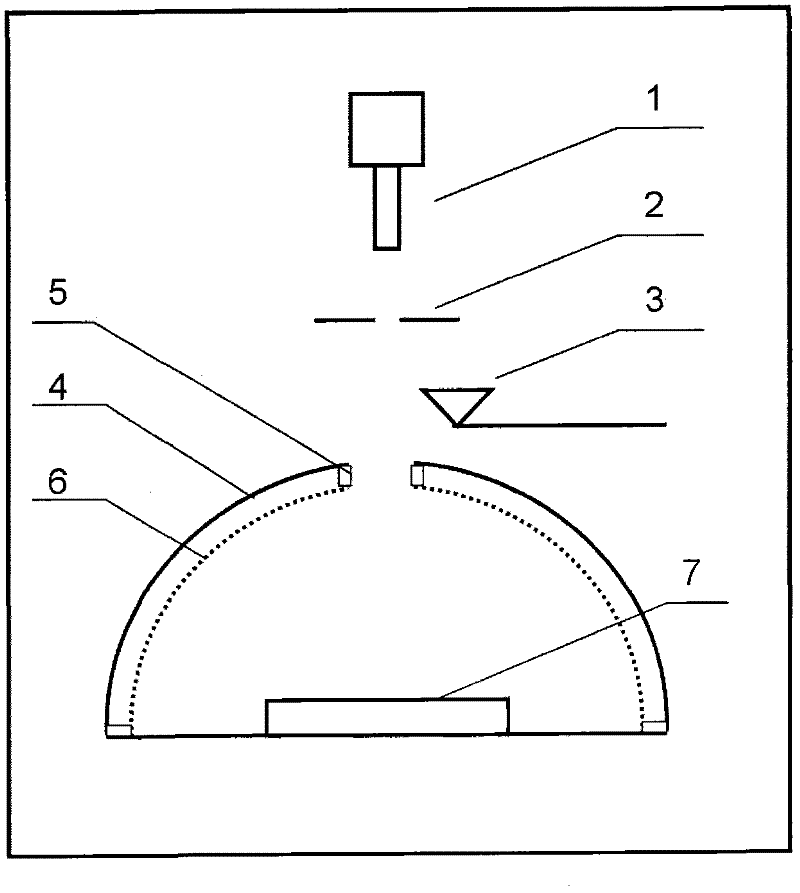
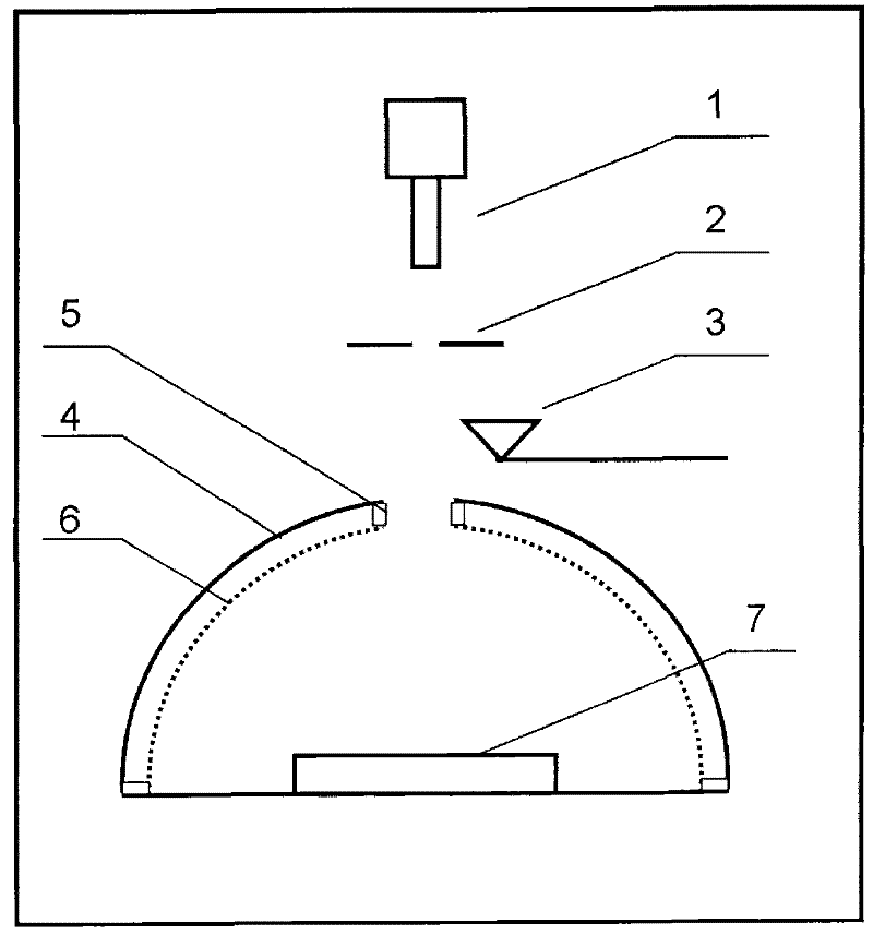
[0020] Such as figure 1 As shown, a test device for distinguishing material secondary electrons and backscattered electrons, said device includes an aperture 2, a Faraday cage 3, a current collector 4, an insulating pad 5, a retardation grid 6 and a sample stage 7. Among them, the aperture 2 is located at the electron emission place of the electron gun 1, and there is a small hole in the middle of the aperture 2 facing the direction of electron emission; the Faraday cage 3 can move freely, and is located behind the aperture 2 when measuring electrons, facing the aperture 2 At the place where the small hole electrons are emitted, the device is withdrawn through the air pressure valve after the measurement is completed; the current collector 4, the insulating pad 5 and the retardation grid 6 together form a semicircular arc with a throu...


PUM

PropertyMeasurementUnit
diameteraaaaaaaaaa
diameteraaaaaaaaaa
thicknessaaaaaaaaaa

Abstract

The invention relates to a testing device for distinguishing secondary electrons and back scattered electrons of a material, and belongs to the technical field of space application. The device comprises a diaphragm, a Faraday cylinder, a current collector, insulation pads, a retarding grid and a sample holder, wherein the diaphragm is positioned at the electron emission port of an electron emission device; the middle of the diaphragm is provided with a small hole; the Faraday cylinder can freely move, is positioned in the rear of the diaphragm when the electrons are measured, and is withdrawnfrom the device after the electrons are measured; a semicircular arc of which the middle is provided with a through hole is formed by the current collector, the insulation pads and the retarding grid; the retarding grid and the current collector are positioned on the inner side and the outer side of the semicircular arc respectively; the insulation pads are positioned on the left and right sides of the through hole respectively; the current collector and the retarding grid on the left part and the current collector and the retarding grid on the right part are connected respectively; and the sample holder opposite to the through hole is positioned at the bottom of the semicircular arc. The device can distinguish the secondary electrons and the back scattered electrons which are generated after primary electrons act with the material, and has the function of analyzing a secondary electron spectrum and a back scattered electron spectrum.

Description

technical field [0001] The invention relates to a test device for distinguishing material secondary electrons and backscattered electrons, belonging to the technical field of space applications. Background technique [0002] The charging and discharging effect of the spacecraft may generate electromagnetic pulses with characteristics of instantaneous high voltage and strong current, causing damage to sensitive electronic components on the spacecraft and misoperation of components, interfering with the communication between the spacecraft and the ground, and even causing the failure of the mission of the spacecraft , Therefore, it is urgent to develop a spacecraft electrification analysis software to evaluate the electrification state of the spacecraft and guide the selection of materials for the anti-static design of the spacecraft. [0003] The developed spacecraft electrification analysis software needs to input the relevant parameters of the analyzed materials, so the acc...

Claims


Application Information

Patent Timeline
Patent Type & Authority Patents(China)
IPC IPC(8): G01N23/22G01N23/203G01R19/00
Inventor 陈益峰李存惠柳青
Owner NO 510 INST THE FIFTH RES INST OFCHINA AEROSPAE SCI & TECH
Learn More