Piezoelectric wafer eigenfrequency measurement method

A technology of piezoelectric wafer and eigenfrequency, which is applied in the field of measurement, can solve the problems of error in measurement results, difficulty in pre-determining, and time-consuming measurement, and achieve the effects of convenient operation, high measurement efficiency, and ingenious structural design

Inactive Publication Date: 2011-06-15
CHINA NAT OFFSHORE OIL CORP +1
View PDF10 Cites 4 Cited by
  • Summary
  • Abstract
  • Description
  • Claims
  • Application Information

AI Technical Summary

Problems solved by technology

[0003] Although the transmission line method can measure the series resonant frequency and parallel resonant frequency of the piezoelectric wafer at the same time, it needs to be carefully adjusted near the characteristic frequency and repeatedly observed the indication value of the high-frequency voltmeter. The measurement is time-consuming and not accurate enough.
And in this measurement method, there are also many limiting conditions, such as requiring the output impedance of the signal generator to be lower than the impedance of the piezoelectric wafer, requiring the impedance of the piezoelectric wafer whose matching resistance is greater than 10 times, etc., and before the measurement, this The impedance value is unknown and difficult to determine in advance. In addition, there are strict requirements on the distributed capacitance of the measurement circuit
Moreover, the transmission line method also has requirements for the size of the sample. For example, for a piezoelectric wafer with a disc-shaped thickness vibration mode, the diameter is required to be much larger than the thickness; for a longitudinally vibrating round rod-shaped piezoelectric wafer, the diameter is required to be much smaller than the length. For piezoelectric wafers with little difference in size, there are often errors in the measurement results by using the transmission line method

Method used


Image

  • Piezoelectric wafer eigenfrequency measurement method
  • Piezoelectric wafer eigenfrequency measurement method
  • Piezoelectric wafer eigenfrequency measurement method

Examples


specific Embodiment

[0025] Such as figure 1 As shown, a PZT-5 rectangular parallelepiped piezoelectric wafer is measured, and its size is 34mm (length L) × 14mm (width W) × 5mm (thickness T). The piezoelectric wafer is polarized in the thickness direction, and an excitation electric field is applied in the thickness direction.

[0026] 1) A device for measuring piezoelectric wafers using the method of the present invention is provided.

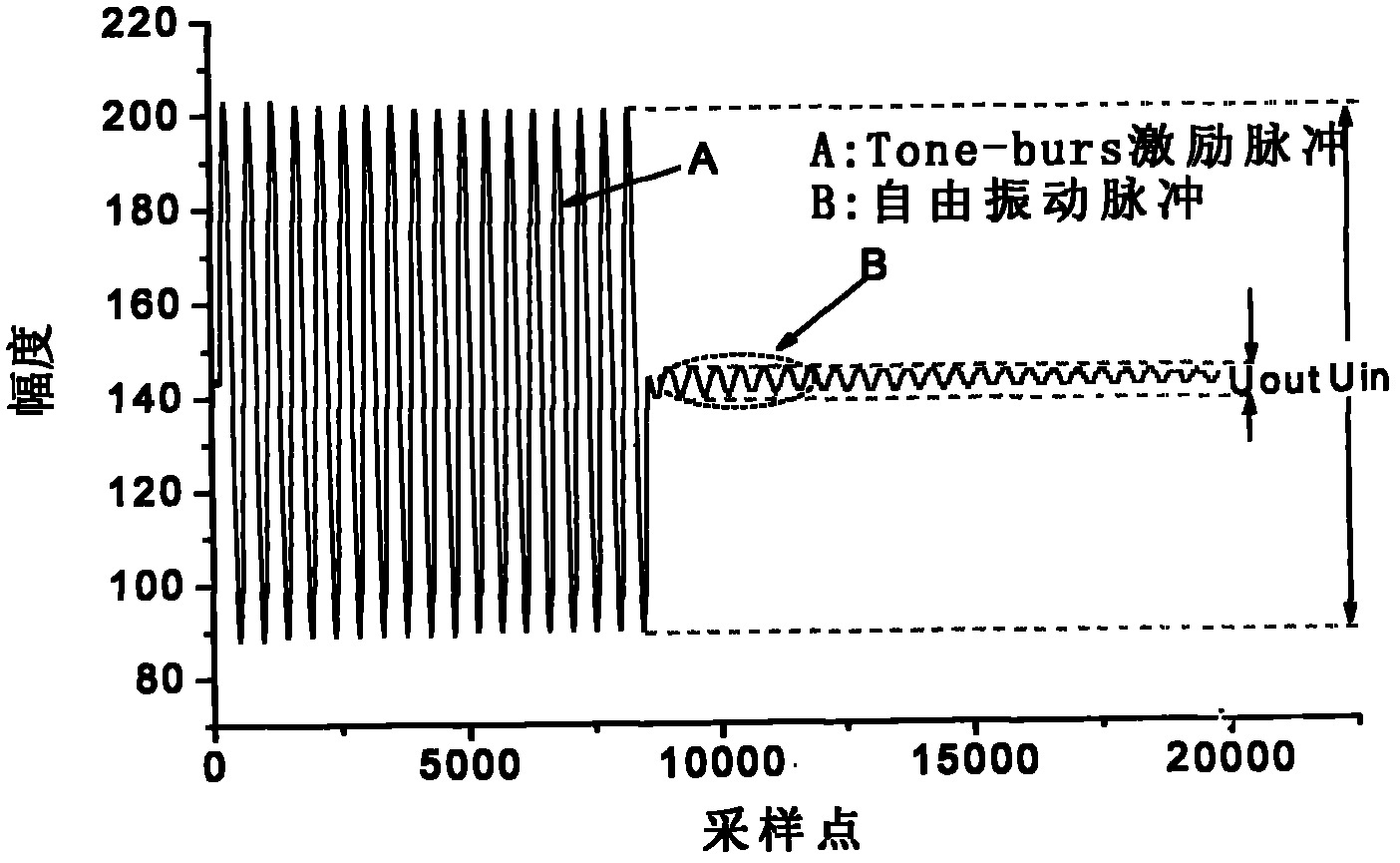
[0027] 2) if figure 2 As shown, the function generator 1 is turned on, and the function generator 1 generates a Tone-Burst sine wave signal A with 18 cycles (the part of the signal indicated by the arrow A in the figure). During this process, the function generator 1 controls the The piezoelectric wafer 2 is excited by electric pulses to make the piezoelectric wafer 2 vibrate. When the function generator 1 completes the number of cycles, the electric pulse excitation to the piezoelectric wafer 2 stops, and the piezoelectric wafer 2 starts to vibrate freely. Di...


PUM


Abstract

The invention relates to a piezoelectric wafer eigenfrequency measurement method. The method comprises the following steps: (1) arranging a measurement device including a function generator, a piezoelectric wafer and a digital oscilloscope; (2) starting the function generator to generate Tone-Burst sine wave signals with a certain period number, conducting electric pulse excitation to the piezoelectric wafer by the function generator at a frequency f, stopping the electric pulse excitation to the piezoelectric wafer when the function generator completes the period number, enabling the piezoelectric wafer to start vibrating freely, and collecting the free vibration signal between two electrodes of the piezoelectric wafer by the digital oscilloscope; (3) adjusting the digital oscilloscope to amplify the free vibration signal between the two electrodes of the piezoelectric wafer in the step (2), and processing the amplified signal by fast Fourier transform; (4) extracting the frequency of the peak on the spectrogram obtained by Fourier transform in the step (3) to obtain the eigenfrequency of the piezoelectric wafer to be tested; and (5) changing the frequency f of the function generator in the step (2), repeating the step (3) and step (4), and measuring each eigenfrequency of the piezoelectric wafer.

Description

technical field [0001] The invention relates to a measuring method, in particular to a measuring method for the eigenfrequency of a piezoelectric wafer. Background technique [0002] Piezoelectric wafers (piezoelectric ceramics) are the core components of sensors such as non-destructive testing ultrasonic probes and seabed sonars in the prior art due to their high electromechanical conversion coefficient and stable performance. Measuring the technical performance parameters such as the eigenfrequency of the piezoelectric wafer is of great significance for selecting a suitable piezoelectric wafer as a sensor. At present, the measurement method of the eigenfrequency of the piezoelectric wafer is mainly the transmission line method. The specific steps are as follows: firstly, a signal generator (also known as a function generator) is used to generate a continuous sine wave electrical signal with adjustable frequency, which is applied to the piezoelectric wafer. In the measurem...

Claims


Application Information

Patent Timeline
IPC IPC(8): G01H11/08
Inventor 曹静蔡桂喜张恩勇周庆祥沙勇董瑞琪刘芳张双楠刘畅
Owner CHINA NAT OFFSHORE OIL CORP
Why Eureka
Try Eureka