Touch control display panel and touch control panel
A touch display panel and touch panel technology, applied in the direction of instruments, electrical digital data processing, data processing input/output process, etc., can solve the problem of increasing the number of control chips, etc., to reduce the number of channels and improve touch sensitivity Effect
- Summary
- Abstract
- Description
- Claims
- Application Information
AI Technical Summary
Problems solved by technology
Method used
Image
Examples
Embodiment Construction
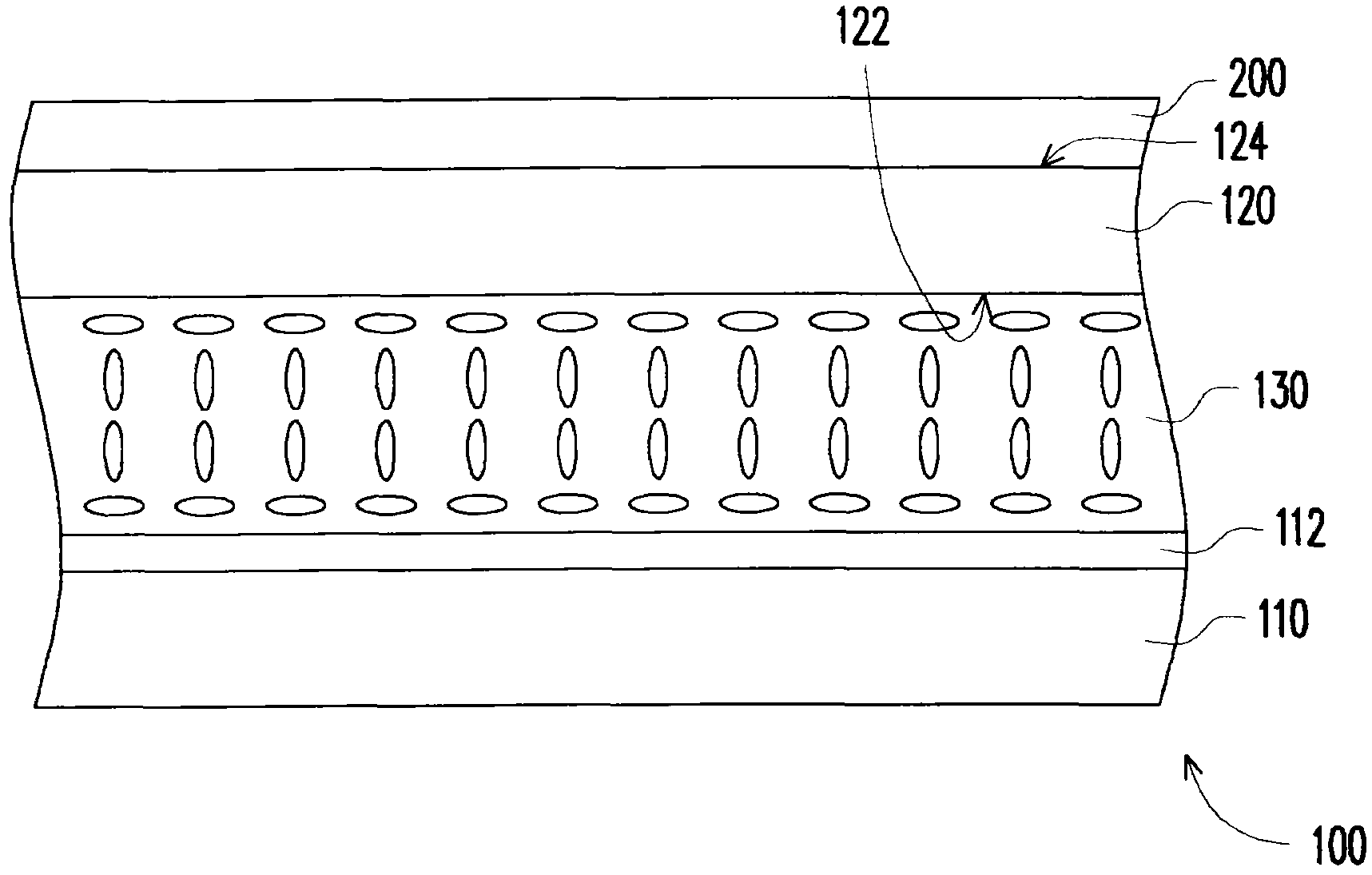
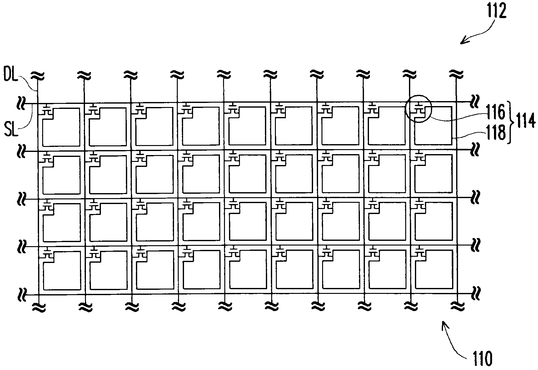
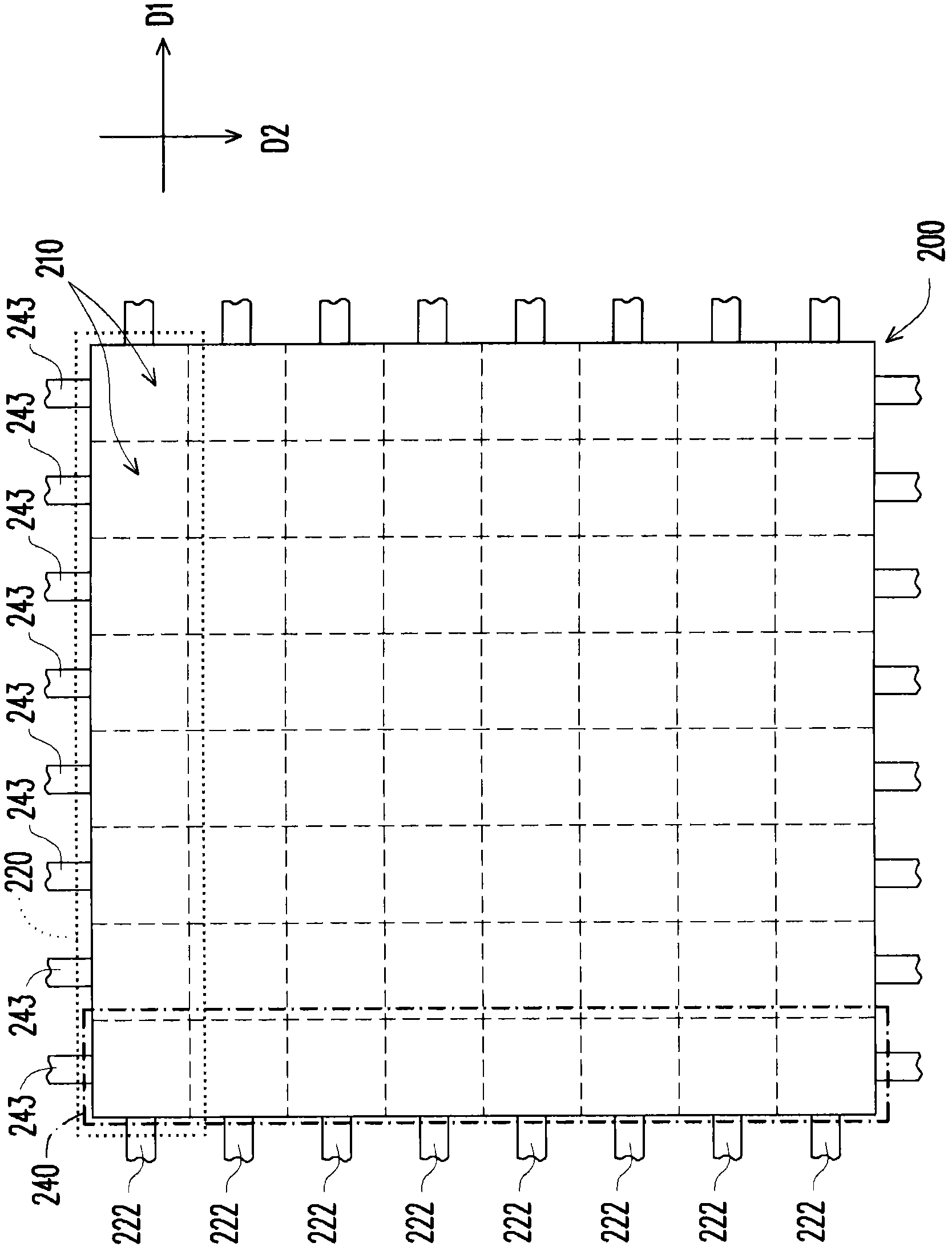
[0065] Figure 1A It is a schematic cross-sectional view of a touch display panel according to an embodiment of the present invention. Figure 1B for Figure 1A A schematic top view of the first substrate. Figure 1C for Figure 1A A schematic top view of the touch electrode layer. Figure 1D for Figure 1C A schematic top view of a sensing area of the touch electrode layer. Figure 1E along Figure 1D Schematic cross-section of the line I-I. Please refer to Figure 1A The touch display panel 100 of this embodiment includes a first substrate 110 , a second substrate 120 , a display medium layer 130 and a touch electrode layer 200 . Wherein, the second substrate 120 is located opposite to the first substrate 110 , wherein the second substrate 120 has an inner surface 122 and an outer surface 124 opposite to the inner surface 122 . The display medium layer 130 is located between the first substrate 110 and the second substrate 120 . The touch electrode layer 200 is locat...
PUM
 Abstract
Description
Claims
Application Information
 - R&D Engineer
- R&D Manager
- IP Professional
- Industry Leading Data Capabilities
- Powerful AI technology
- Patent DNA Extraction
Browse by: Latest US Patents, China's latest patents, Technical Efficacy Thesaurus, Application Domain, Technology Topic, Popular Technical Reports.
© 2024 PatSnap. All rights reserved.Legal|Privacy policy|Modern Slavery Act Transparency Statement|Sitemap|About US| Contact US: help@patsnap.com


