Electro-optic modulator based on gamma 51 and realization method
An electro-optic modulator and electro-optic crystal technology, which is applied in the fields of instruments, optics, nonlinear optics, etc., can solve the problems of seldom used and inconvenient to use
- Summary
- Abstract
- Description
- Claims
- Application Information
AI Technical Summary
Problems solved by technology
Method used
Image
Examples
Embodiment 1
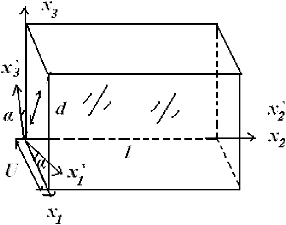
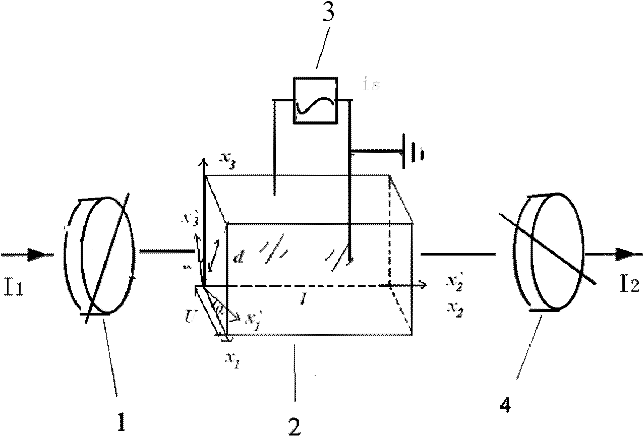
[0035] Embodiment one, according to figure 1 Cut KTa 0.35 Nb 0.65 o 3 Crystal, when l=1mm, d=1mm, l is the length of the crystal in the direction, d is the length of the crystal in the direction, near room temperature T=28°C, light wave wavelength λ=0.633μm, the half-wave voltage U π is 118V. Realize electro-optic modulation.
Embodiment 2
[0036] Embodiment two, according to figure 1 Cut BaTiO 3 Crystal, when l=1cm, d=1mm, l is the length of the crystal in the direction, d is the length of the crystal in the direction, at room temperature T=28°C, λ=0.546μm, the half-wave voltage U π =234V, realizing electro-optic modulation.
Embodiment 3
[0037] Example 3: Thin-film technology will be used to grow a-axis epitaxial growth of μm-level KTa on a platinum-coated Si substrate 0.35 Nb 0.65 o 3 Thin film, take l=1mm, d=2μm, the width of the sample is taken as 1mm, l is the length of the direction crystal, d is the length of the direction crystal; when T=28℃ near room temperature, λ=0.633μm, Half wave voltage U π It is 0.3V to realize electro-optic modulation.
PUM
 Abstract
Description
Claims
Application Information
 - Generate Ideas
- Intellectual Property
- Life Sciences
- Materials
- Tech Scout
- Unparalleled Data Quality
- Higher Quality Content
- 60% Fewer Hallucinations
Browse by: Latest US Patents, China's latest patents, Technical Efficacy Thesaurus, Application Domain, Technology Topic, Popular Technical Reports.
© 2025 PatSnap. All rights reserved.Legal|Privacy policy|Modern Slavery Act Transparency Statement|Sitemap|About US| Contact US: help@patsnap.com


