Electron-emitting device and electron source, electron beam apparatus as well as image display apparatus using the same
A technology of electron emission and devices, which is applied in the direction of image/graphic display tubes, cathode ray tubes/electron beam tubes, electrical components, etc., can solve the problems of improving stability over time and achieve the effect of minimizing production
- Summary
- Abstract
- Description
- Claims
- Application Information
AI Technical Summary
Problems solved by technology
Method used
Image


Examples
no. 1 example
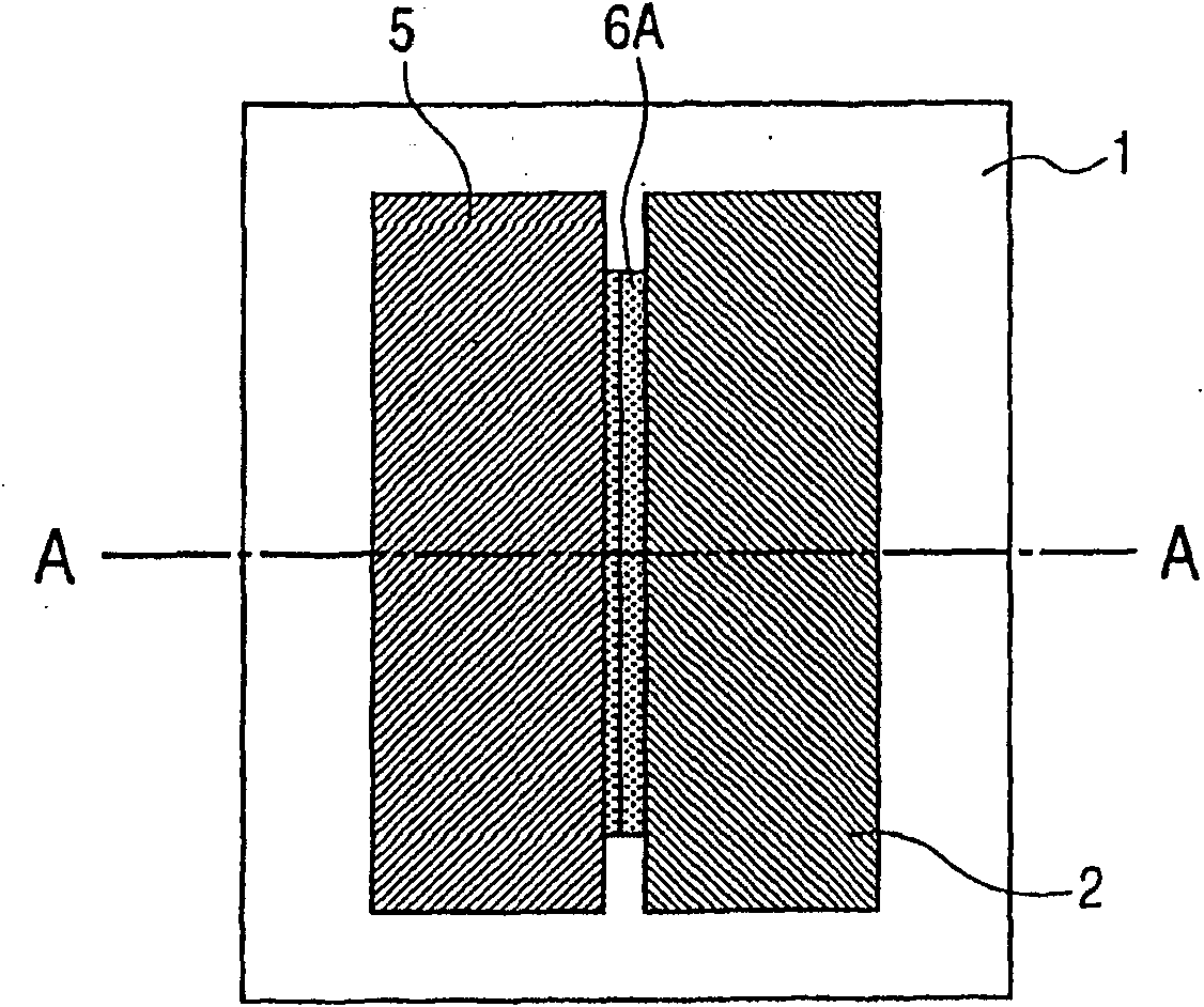
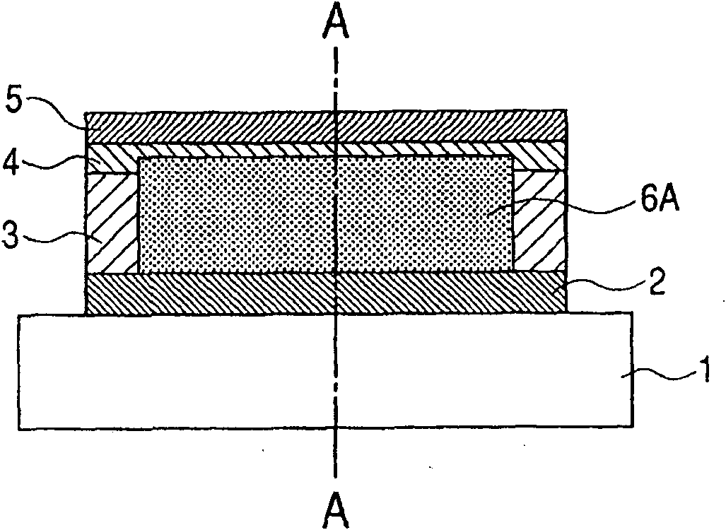
[0134] Figure 1A is a schematic plan view of an electron-emitting device according to an embodiment of the present invention. Figure 1B is along Figure 1A The section taken by the line A-A. Figure 1C From Figure 1B A side view of the device viewed from the direction indicated by the arrow in .
[0135] exist Figure 1A , Figure 1B and Figure 1C , the insulating layers 3 and 4 form an insulating member. In this embodiment, this member forms steps on the surface of the substrate 1 . The gate electrode 5 is located on the insulating member. The cathode 6A is formed of a conductive material, is electrically connected to the electrode 2, is located on the outer surface of the insulating layer 3 as a part of the insulating member forming a step, and has a protruding portion serving as an electron emission portion. Recessed portion (recess) 7 is formed such that the side of insulating layer 4 is retracted inwardly to be recessed relative to the side (outer surface) of in...
no. 2 example
[0158] Figure 13A is a schematic plan view of an electron-emitting device according to an embodiment of the present invention. Figure 13B is along Figure 13A The section taken by the line A-A. Figure 13C From Figure 13A A side view of the device when viewed from the direction indicated by the arrow in .
[0159] exist Figure 13A , Figure 13B and Figure 13C In , the insulating layers 3 and 4 form insulating members and form steps on the surface of the substrate 1 . Gate electrode 5 is located on the outer surface of the insulating member (upper surface of insulating layer 4 ). The strip-shaped cathodes 60A1 to 60A4 are electrically connected to the electrode 2 and provided on the outer surface of the insulating layer 3 which is a part of the insulating member forming a step. The recessed portion 7 is formed such that the sides of the insulating layer 4 are retracted inwardly to be recessed relative to the outer surface (side) of the insulating layer 3 and the si...
no. 3 example
[0170] Figure 14Ais a schematic plan view of an electron-emitting device according to an embodiment of the present invention. Figure 14B is along Figure 14A The section taken by the line A-A. Figure 14C From Figure 14A A side view of the device when viewed from the direction indicated by the arrow in .
[0171] exist Figure 14A , Figure 14B and Figure 14C In , the insulating layers 3 and 4 form insulating members and form steps on the surface of the substrate 1 . The gate electrode 5 is located on the outer surface of the insulating member (on the insulating layer 4 forming a part of the insulating member). Strip electrode 6A is formed of a conductive material, is electrically connected to electrode 2 , and is provided on the outer surface of insulating layer 3 that is a part of the insulating member. A humped portion 6B of the gate electrode is formed of the same material as that used to form the cathode of the electron emission portion, and is connected to th...
PUM
 Abstract
Description
Claims
Application Information
 - R&D
- Intellectual Property
- Life Sciences
- Materials
- Tech Scout
- Unparalleled Data Quality
- Higher Quality Content
- 60% Fewer Hallucinations
Browse by: Latest US Patents, China's latest patents, Technical Efficacy Thesaurus, Application Domain, Technology Topic, Popular Technical Reports.
© 2025 PatSnap. All rights reserved.Legal|Privacy policy|Modern Slavery Act Transparency Statement|Sitemap|About US| Contact US: help@patsnap.com