Solid-state image pickup element and a method of manufacturing the same, and image pickup device including the same

A technology of an imaging element and a manufacturing method, which is applied to radiation control devices, electrical components, electric solid-state devices, etc., to achieve the effects of stable operation and excellent image quality

Active Publication Date: 2011-03-23
SONY GRP CORP
View PDF5 Cites 6 Cited by
  • Summary
  • Abstract
  • Description
  • Claims
  • Application Information

AI Technical Summary

Problems solved by technology

[0009] However, from the viewpoint of sufficiently ensuring the characteristics of the solid-state imaging element, etc., it is not desirable to keep the high temperature for a long time

Method used


Image

  • Solid-state image pickup element and a method of manufacturing the same, and image pickup device including the same
  • Solid-state image pickup element and a method of manufacturing the same, and image pickup device including the same
  • Solid-state image pickup element and a method of manufacturing the same, and image pickup device including the same

Examples


Embodiment Construction

[0039] Hereinafter, preferred embodiments of the present invention will be described in detail with reference to the accompanying drawings.

[0040] It should be noted that the following will be described in the following order.

[0041] 1. Outline of the present invention

[0042] 2. Solid-state image sensor

[0043] 3. Manufacturing method of solid-state imaging device

[0044] 4. Experiment (measurement of characteristics)

[0045] 5. Camera device

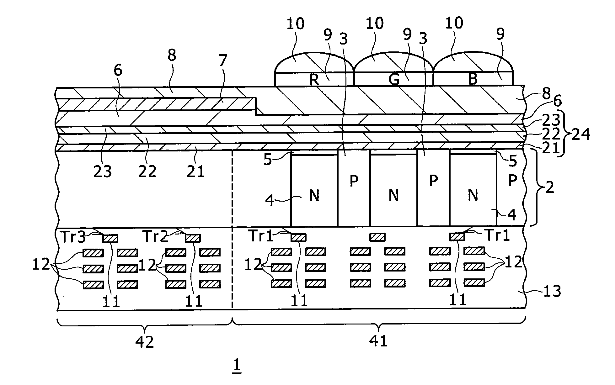
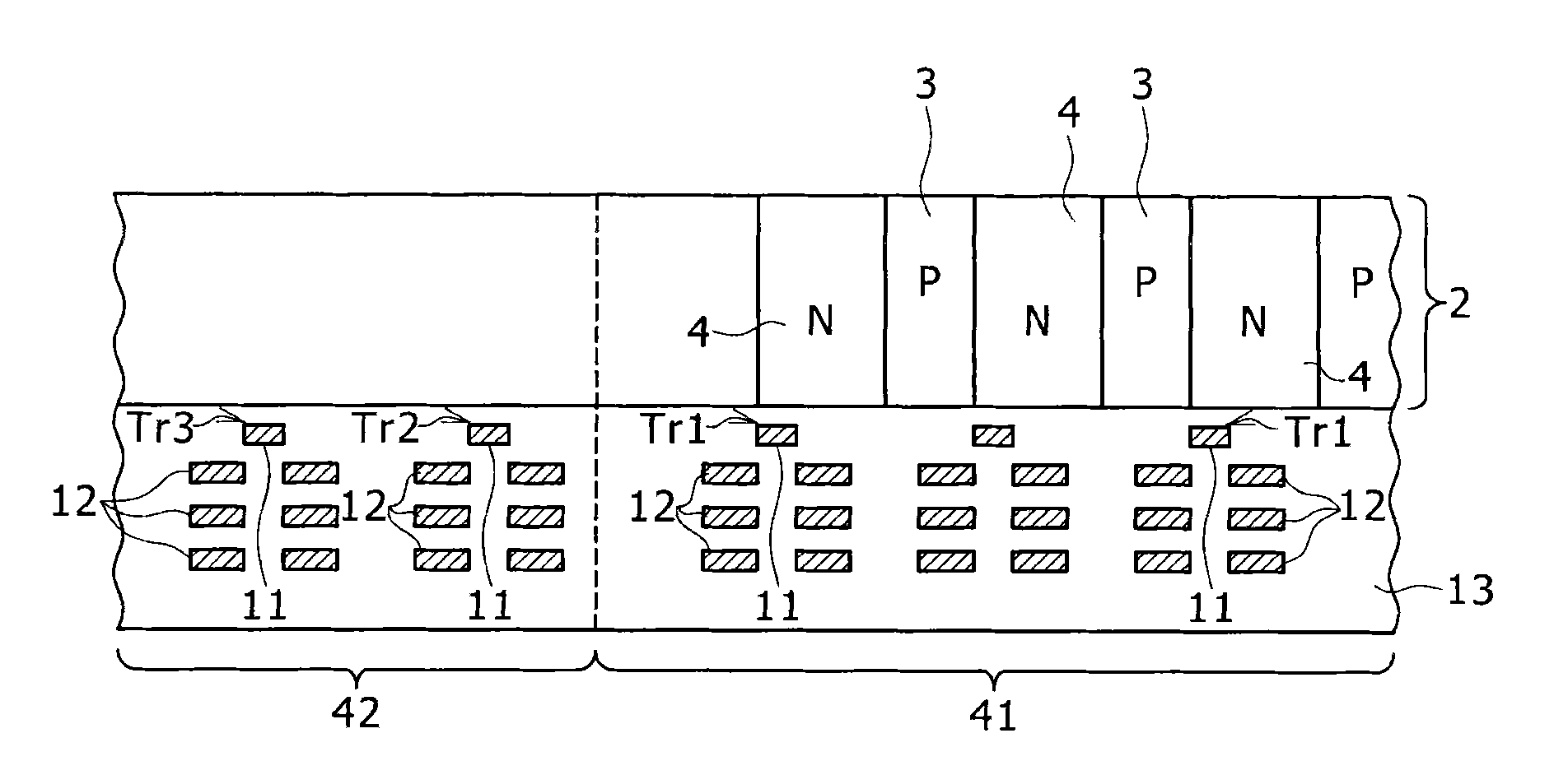
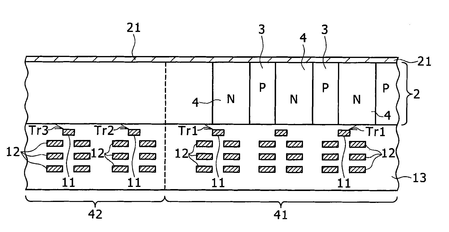
[0046] 1. Outline of the present invention

[0047] In the present invention, a first film in which negative fixed charges are contained is formed on the semiconductor layer in at least a region where a photodiode of a solid-state imaging element is formed, and a second film in which negative fixed charges are contained is formed on the first film. In addition, a third film containing negative fixed charges therein is formed on the second film.

[0048] The first film is formed (deposited) using an atomic layer deposition...


PUM


Abstract

The invention provides a solid-state image pickup element and a method of manufacturing the same and an image pickup device including the same. The solid-state image pickup element, includes: a semiconductor layer in which a photodiode for carrying out photoelectric conversion is formed; a first film containing negative fixed charges and formed on the semiconductor layer in a region in which at least the photodiode is formed by utilizing either an atomic layer deposition method or a metal organic chemical vapor deposition method; a second film containing the negative fixed charges and formed on the first film containing therein the negative fixed charges by utilizing a physical vapor deposition method; and a third film containing the negative fixed charges and formed on the second film containing therein the negative fixed charges by utilizing either the atomic layer deposition method or the metal organic chemical vapor deposition method.

Description

technical field [0001] The present invention relates to a solid-state imaging element, a manufacturing method thereof, and an imaging device including the solid-state imaging element. Background technique [0002] In a CCD (Charge Coupled Device) solid-state imaging element and a CMOS (Complementary Metal Oxide Semiconductor) solid-state imaging element, it is known that crystal defects occurring in the photodiode and in the light-receiving portion formed in the silicon substrate and the overlying light An interface state in the interface between the insulating layers of the receiving portion causes dark current. [0003] Figure 13A is a schematic cross-sectional view showing a state where an insulating layer is formed on a silicon layer in which a photodiode is formed, and Figure 13B yes Figure 13A Energy diagrams for insulating and silicon layers are shown. Therefore, if Figure 13A and 13B As shown, interface states each indicated by a mark x are generated in the in...

Claims


Application Information

Patent Timeline
Patent Type & Authority Applications(China)
IPC IPC(8): H01L27/146H04N5/335H04N5/225
CPCH01L27/14601H01L27/14621H01L27/14632H01L27/14645H01L27/14627H01L27/14689H01L27/14692
Inventor 押山到宫田英治
Owner SONY GRP CORP
Why Eureka
Try Eureka