
Transflective liquid crystal display

A semi-transmissive semi-reflective, liquid crystal display device technology, applied in the direction of instruments, nonlinear optics, optics, etc., can solve the problems of white or black embossing, long response time, color shift, etc., to slow down the color shift, slow down pressure The effect of streaking

Inactive Publication Date: 2011-03-23
WINTEK CORP
View PDF0 Cites 1 Cited by
  • Summary
  • Abstract
  • Description
  • Claims
  • Application Information

AI Technical Summary

Problems solved by technology

[0004] In addition, existing liquid crystal displays using a vertical alignment structure may have color washout when viewed from a large viewing angle.
In addition, when the existing liquid crystal display is touched with a finger, white or black embossing (ie, finger print mura) phenomenon occurs due to the state of the liquid crystal being disturbed
Generally, the response time for the messy liquid crystal state in the existing liquid crystal display to return to the original state of dumping along the direction of the electric field is relatively long, so that the embossing phenomenon can be observed by the human eye.

Method used


Image

  • Transflective liquid crystal display
  • Transflective liquid crystal display
  • Transflective liquid crystal display

Examples


Embodiment Construction

[0067] In order to make the object, technical solution and advantages of the present invention clearer, the embodiments of the present invention will be further described in detail below in conjunction with the accompanying drawings. Here, the exemplary embodiments and descriptions of the present invention are used to explain the present invention, but not to limit the present invention.

[0068] Here, it should be noted that the term "A layer is formed on the B layer" in this specification is not limited to the way that the A layer directly touches the surface of the B layer. For example, there is a gap between the A layer and the B layer. the scope covered by this term.

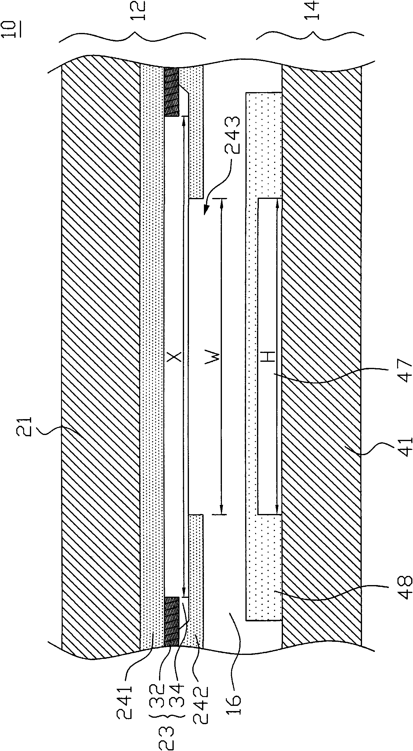
[0069] figure 2 It is a schematic diagram of a partial section of a transflective liquid crystal display according to an embodiment of the present invention. Such as figure 2 As shown, the transflective liquid crystal display 10 includes a filter substrate 12 and an active component substrate 14 facing...


PUM


Abstract

The invention discloses a transflective liquid crystal display comprising an active assembly substrate, a colorful filter substrate and a liquid crystal layer, wherein the active assembly substrate comprises a first transparent substrate, a plurality of switching assemblies, a plurality of transparent pixel electrodes and a plurality of reflected pixel electrodes, and the switching assemblies, the transparent pixel electrodes and the reflected pixel electrodes are formed on the first transparent substrate; and the colorful filter substrate comprises a second transparent substrate, a first transparent conducting layer, a second transparent conducting layer and a dielectric layer, wherein the first transparent conducting layer is positioned between the second transparent substrate and the second transparent conducting layer, the dielectric layer is positioned between the first transparent conducting layer and the second transparent conducting layer, the second transparent conducting layer in each pixel region defines at least one opening, and the opening respectively corresponds to the reflected pixel electrode. By the implementation of the transflective liquid crystal display, the Gamma curves of a penetration region and a reflecting region can be adjusted to better Gamma curves, and the phenomena of color offset and embossing are effectively alleviated.

Description

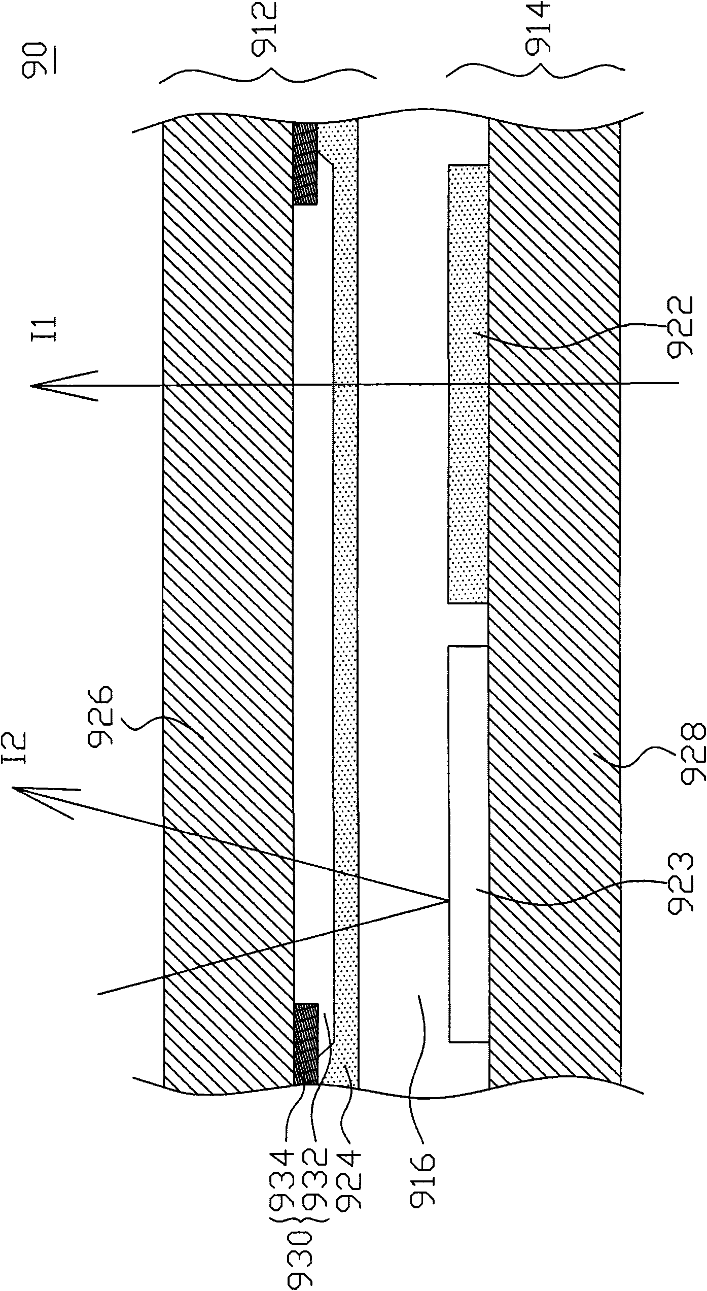
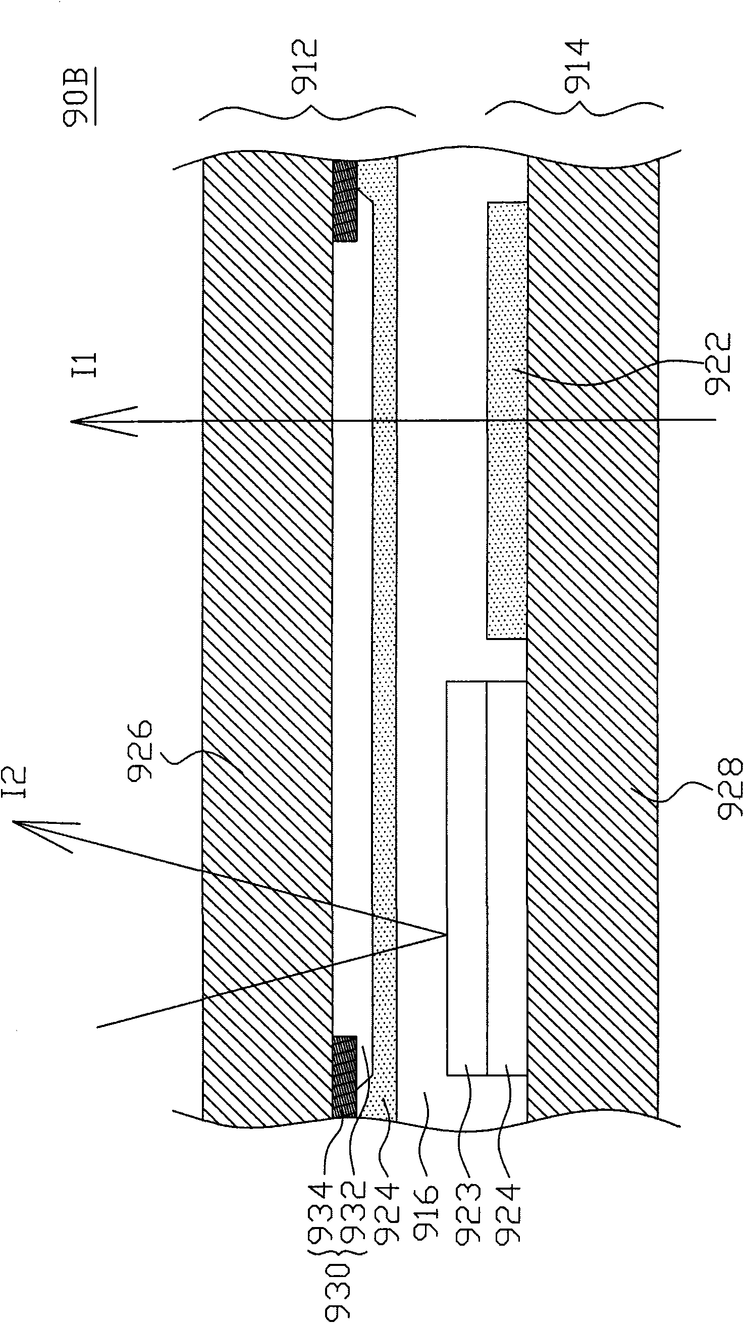
technical field [0001] The invention relates to a transflective liquid crystal display, in particular to a transflective liquid crystal display capable of adjusting the Gamma curves of the transmissive area and the reflective area to a better Gamma curve. Background technique [0002] Figure 1A It is a schematic diagram of a partial section of an existing transflective liquid crystal display. Such as Figure 1A As shown, the transflective liquid crystal display 90 includes a filter substrate 912 and an active component substrate 914 facing each other, and a liquid crystal layer 916 is interposed between the two substrates. The liquid crystal layer 916 adopts a negative dielectric anisotropy liquid crystal material, so that the liquid crystal molecules are vertically aligned when no voltage is applied. On the transparent substrate 928 of the active device substrate 914 are formed a switching device (not shown), such as a thin film transistor (TFT), a transparent electrode 9...

Claims


Application Information

Patent Timeline
IPC IPC(8): G02F1/1335G02F1/1362
Inventor 王文俊游明璋张永政
Owner WINTEK CORP
Learn More