Internal board structure for printed circuit board

A technology for printed circuit boards and inner-layer boards, applied to printed circuit components, circuit substrate materials, etc., can solve problems such as poor wrinkles and lack of glue, and achieve the effects of convenient pressing, sufficient glue filling, and improved production quality

Inactive Publication Date: 2011-02-02
昆山元茂电子科技有限公司
View PDF2 Cites 4 Cited by
  • Summary
  • Abstract
  • Description
  • Claims
  • Application Information

AI Technical Summary

Problems solved by technology

[0003] The inner layer boards of many material numbers in the existing factory have the following designs: broken edges, large Dummy PAD area, partitioned PAD in the scraping glue area, etc., all of which have copper-free areas. Because the glue is fluid during the lamination process, it will Make part of the glue to fill the above copper-free area, so in the actual lamination process, due to the large and many Dummy PAD areas, it is easy to cause insufficient glue filling and lack of glue, resulting in poor wrinkles

Method used


Image

  • Internal board structure for printed circuit board
  • Internal board structure for printed circuit board
  • Internal board structure for printed circuit board

Examples


Embodiment Construction

[0014] In order to make the technical means, creative features, goals and effects achieved by the present invention easy to understand, the present invention will be further described below in conjunction with specific embodiments.

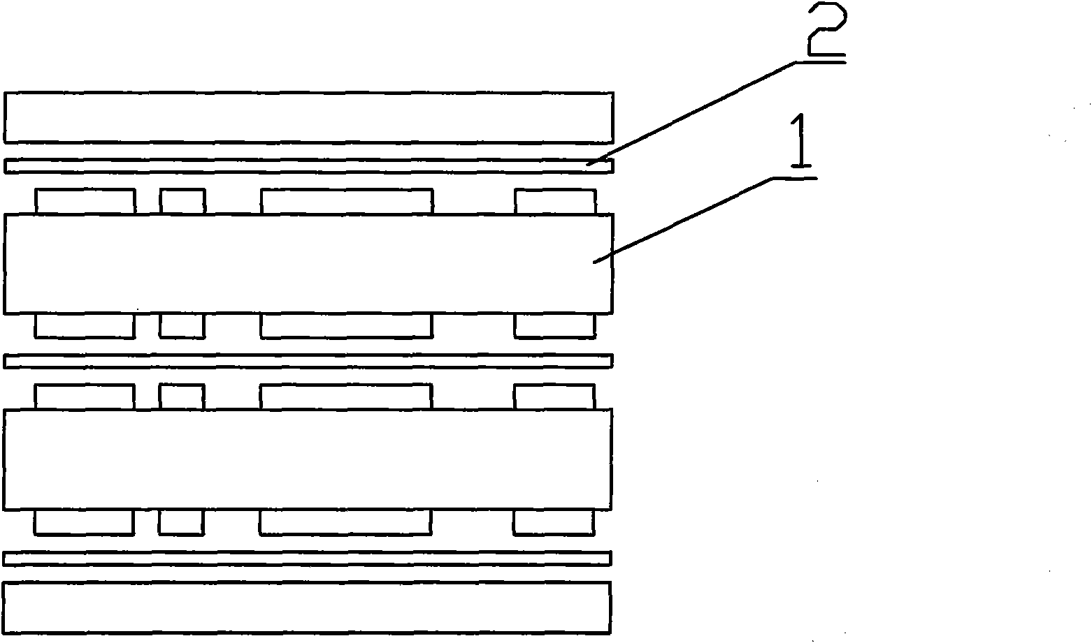
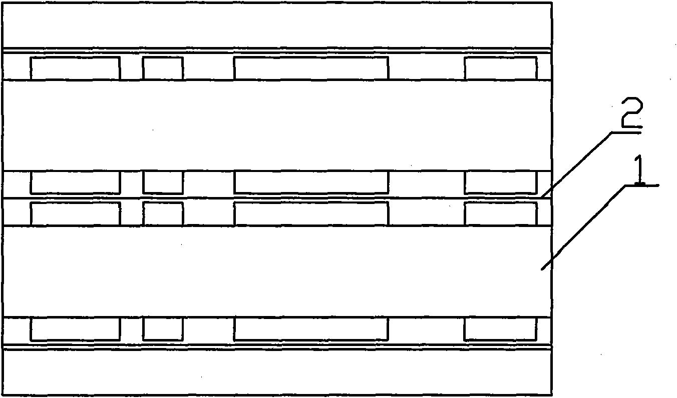
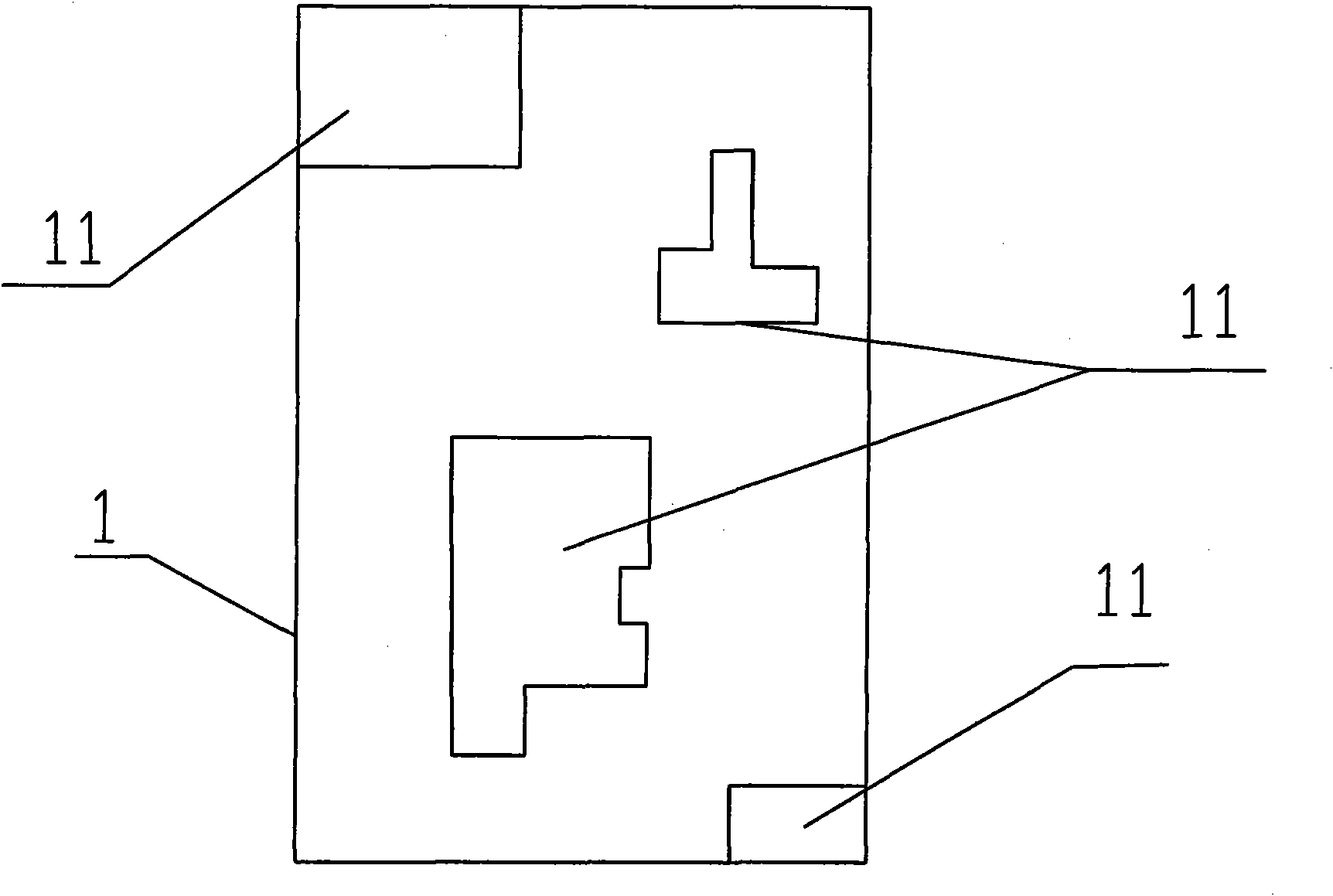
[0015] see Figure 1 to Figure 3 , this embodiment provides an inner board structure applied to printed circuit boards, including an inner board 1 and a scraping glue area 11 arranged on the inner board 1; the surface of the scraping glue area 11 is fully plated There is a copper layer; the upper and lower panels of the inner layer board 1 are laminated with a film 2; the inner layer board 1 adopts an all-copper structure to avoid the fluidity of the glue during the lamination process, which will cause part of the glue to fill up above the copper-free area.

[0016] In this embodiment, the film 2 is a resin film. In this implementation, multiple inner boards with circuits are passed through the press, and the resin film is used to bond them toget...


PUM


Abstract

The invention discloses an internal board structure for a printed circuit board, which comprises an internal board and a flowing adhesive scrapping area arranged on the internal board, and is characterized in that: the entire surface of the flowing adhesive scraping area is plated with a copper layer; and both the upper and lower panels of the internal board are laminated with an adhesive piece. In the invention, the surface of the flowing adhesive area of the internal board is modified into an all-copper structure, so in the laminating process, the adverse phenomenon that part of the adhesive which is flowable flows to the areas without copper and generate wrinkles is eliminated; enough adhesive is filled, the laminating is convenient and quick, and the production quality of the internal board is improved.

Description

technical field [0001] The invention relates to the technical field of lamination of printed circuit boards, in particular to an inner layer board structure applied to printed circuit boards. Background technique [0002] With the popularization and wide application of electronic products, the production and manufacturing technology of printed circuit board (Print Circuit board referred to as PCB board) is constantly updated and developed. In order to meet the needs of producing different electronic products, the design and application of PCB boards have been developed from single-layer boards to double-layer boards or multi-layer boards. [0003] Many material numbers in the existing factory have the following designs for inner layer boards: broken edges, large Dummy PAD area, partitioned PAD in the scraping glue area, etc., all of which have copper-free areas. Because the glue is fluid during the lamination process, it will Make part of the glue to fill the above copper-f...

Claims


Application Information

Patent Timeline
Patent Type & Authority Applications(China)
IPC IPC(8): H05K1/03
Inventor 田锋韩业刚
Owner 昆山元茂电子科技有限公司
Why Eureka
Try Eureka