
Device for controlling power transistor

A transistor, bipolar transistor technology, applied in the direction of transistors, semiconductor devices, output power conversion devices, etc., can solve the problems of limited minimum turn-on voltage range of transistors, unsuitable for controlling JFET transistors, etc., to control switching losses. Effect

Inactive Publication Date: 2014-12-17
SCHNEIDER TOSHIBA INVERTER EUROPE SAS
View PDF5 Cites 0 Cited by
  • Summary
  • Abstract
  • Description
  • Claims
  • Application Information

AI Technical Summary

Problems solved by technology

However, this device is still not suitable for controlling JFET-type transistors
In practice, in a JFET, the voltage range between the minimum turn-on voltage and the maximum voltage that a transistor can support is very limited

Method used


Image

  • Device for controlling power transistor
  • Device for controlling power transistor
  • Device for controlling power transistor

Examples


Embodiment Construction

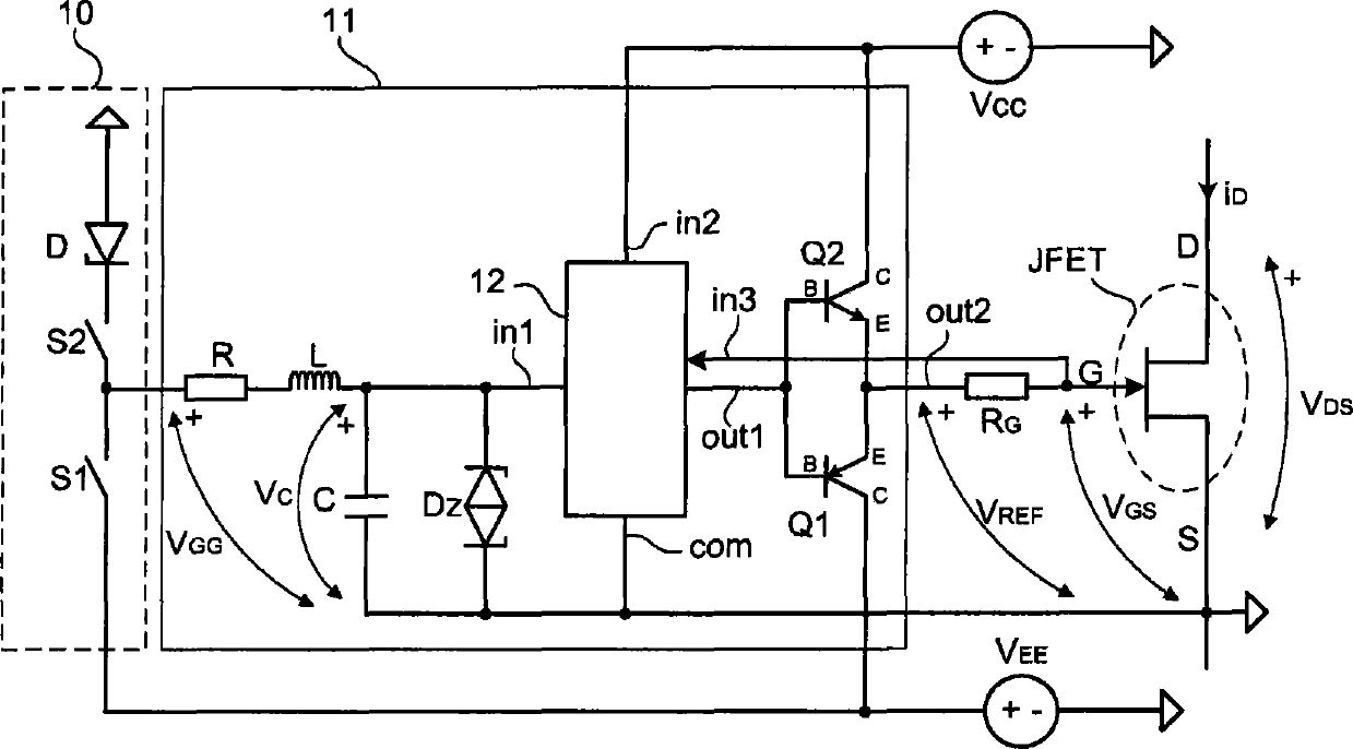
[0027] The device of the invention is suitable for the control of transistors of the JFET (Junction Field Effect Transistor) type.

[0028] JFET transistors are known power electronic switches that include a control gate (G) whose function is to enable or prevent current from passing between a drain (D) and a source (S). If the voltage between the gate and source V GS Close to zero, then such a transistor is normally on (ON type). This means that the control voltage V GS When absent, the drain-source path is flow-through or conducting. Conversely, if there is no voltage V between the gate and source GS When the drain-source path is not conducting, the JFET transistor is normally off type (OFF type).

[0029] According to the present invention, the controlled JFET transistor will preferably be made of a wide bandgap material such as silicon carbide or gallium nitride, so as to exhibit a low impedance (R DSon ), thus producing limited losses and withstanding high voltages (...


PUM


Abstract

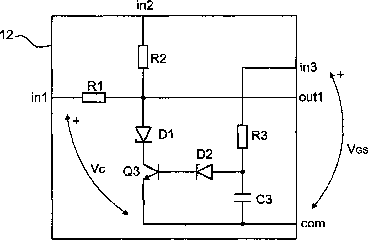
#CMT# # / CMT# The device has a voltage generation circuit (11) comprising an output terminal (out-1) connected with a gate of a Junction FET and generating reference gate-source voltage (VREF) at the output terminal. A voltage limiting circuit (12) limits the reference gate-source voltage to a predetermined maximum value when gate-source voltage (VGS) at a terminal of the Junction FET exceeds the maximum value. A clamping diode (Dz) is arranged between an input terminal (in1) of the limiting circuit and a source of the Junction FET. #CMT#USE : # / CMT# Gate control device for controlling a Junction FET in a power converter (claimed). #CMT#ADVANTAGE : # / CMT# The device is designed such that performance characteristic of the Junction FET is optimized to reduce switching losses and electromagnetic interference when the Junction FET is switched ON. #CMT#DESCRIPTION OF DRAWINGS : # / CMT# The drawing shows a circuit representation of a gate control device for a Junction-FET. Dz : Clamping diode in1-in3 : Input terminals out-1, out-2 : Output terminals VGS : Transistor gate-source voltage VREF : Reference gate-source voltage 11 : Voltage generation circuit 12 : Voltage limiting circuit.

Description

technical field [0001] This invention relates to control devices for power transistors, and more particularly to junction field effect crystal JFETs. JFET transistors will be made, for example, from high bandgap energy materials such as silicon carbide or gallium nitride. Such transistors can be used in particular in inverters with pulse width modulation (PWM). Background technique [0002] Many publications have been written on the control of transistors, especially of the IGBT (Insulated Gate Bipolar Transistor) type. [0003] In the control of transistors, the main problem to be solved is how to control the switching speed of transistors. To this end, it is essential to be able to control the change in current over time (di / dt) and the change in voltage over time (dV / dt) independently of each other. When the transistor is on, the aim is eg to reduce di / dt and increase dV / dt. However, the known control functions are not satisfactory in most cases. [0004] Petar J. Gr...

Claims


Application Information

Patent Timeline
Patent Type & Authority Patents(China)
IPC IPC(8): H02M1/08
CPCH03K17/163H03K17/08122
Inventor 皮塔·格尔波维克
Owner SCHNEIDER TOSHIBA INVERTER EUROPE SAS
Learn More