
Variable resistance memory device

A resistance storage, variable technology, applied in information storage, static memory, read-only memory, etc., can solve problems such as hindering high-speed operation, and achieve the effect of reducing size

Inactive Publication Date: 2010-07-28
SONY GRP CORP
View PDF4 Cites 19 Cited by
  • Summary
  • Abstract
  • Description
  • Claims
  • Application Information

AI Technical Summary

Problems solved by technology

This hinders high-speed operation

Method used


Image

  • Variable resistance memory device
  • Variable resistance memory device
  • Variable resistance memory device

Examples


no. 1 approach

[0066] 1. First Embodiment: Driving an N-type (common line transfer transistor) PT ( Figure 5 and Figure 6 )

[0067] 2. Second Embodiment: Driving an N-type PT ( Figure 7 and Figure 8 )

no. 3 approach

[0068] 3. Third Embodiment: Driving a P-type PT in a grounded state of the drain ( Figure 9 and Figure 10 )

[0069] 4. The fourth embodiment: driving the P-type PT in the Vdd connection state of the source ( Figure 11 and Figure 12 )

no. 5 approach

[0070] 5. The fifth embodiment: specific IC structure and control example ( Figure 13 ~ Figure 2 9)

[0071] 6. The first modified example: BL driver configuration example 1 ( Figure 30 )

[0072] 7. The second modified example: BL driver configuration example 2 ( Figure 31 )

[0073] 8. The third modified example: WL driver configuration example ( Figure 34 )

[0074] 1. First Embodiment

[0075] storage unit structure

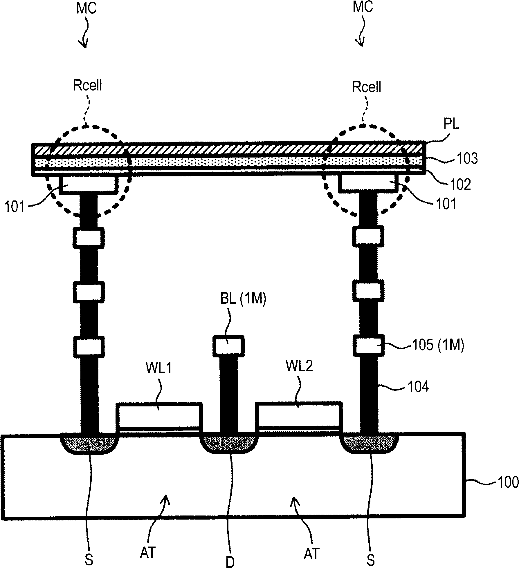
[0076] exist Figure 1A and Figure 1B An equivalent circuit of a memory cell common to various embodiments of the present invention is shown in . exist Figure 1A The direction of the write current is shown in . exist Figure 1B The direction of the erase current is shown in . However, the memory cell configuration itself is common to both figures.

[0077] Figure 1A and Figure 1B The memory cell MC includes a variable cell resistor Rcell and an access transistor AT as a "memory element".

[0078] One end of the variable cell resistor Rce...


PUM


Abstract

A variable resistance memory device includes: a first common line; a second common line; plural memory cells each formed by serially connecting a memory element, resistance of which changes according to applied voltage, and an access transistor between the second common line and the first common line; a common line pass transistor connected between the first common line and a supply node for predetermined voltage; and a driving circuit that controls voltage of the second common line, the predetermined voltage, and voltage of a control node of the common line pass transistor and drives the memory cells. According to the invention, the variable resistance memory device can control the size of the drive circuit and make the high-speed operation possible.

Description

[0001] Cross References to Related Applications [0002] The present application contains subject matter related to that disclosed in Japanese Priority Patent Application JP 2009-012385 filed in the Japan Patent Office on Jan. 22, 2009, the entire content of which is hereby incorporated by reference. technical field [0003] The present invention relates to a variable resistance memory device in which each memory cell is formed by connecting a memory element whose resistance changes according to an applied voltage and an access transistor in series. Background technique [0004] There is known a variable resistance memory device having a memory element for each memory cell, wherein the resistance of the memory element changes according to the implantation of conductive ions into or the removal of conductive ions from the insulating layer (for example, see K "A Novel Resistance Memory with High Scalability and Nanosecond Switching" by Aratani et al., Technical Digest IEDM 200...

Claims


Application Information

Patent Timeline
Patent Type & Authority Applications(China)
IPC IPC(8): G11C16/02G11C16/24
CPCG11C13/0069G11C2213/79G11C2213/11G11C2213/33G11C11/56G11C13/0009G11C2213/34G11C2213/56G11C2013/0073G11C13/0064
Inventor 北川真椎本恒则大塚渉
Owner SONY GRP CORP
Learn More