
Pad connecting structure, lead wire jointing structure and encapsulating structure

A technology of packaging structure and pad structure, which is applied in the direction of semiconductor devices, semiconductor/solid-state device components, electrical components, etc., can solve problems such as stress concentration, peeling of bonding wire 910 and pad 920, damage and deformation, and reduce damage or Deformation, reduce peeling problems, and ensure the effect of bonding quality

Inactive Publication Date: 2010-06-23
ASE ASSEMBLY & TEST SHANGHAI
View PDF0 Cites 4 Cited by
  • Summary
  • Abstract
  • Description
  • Claims
  • Application Information

AI Technical Summary

Problems solved by technology

At present, the copper bonding wire 910 can be bonded to the pad 920 by a wire bonding machine 901. However, when the hardness of the copper bonding wire 910 is greater than the hardness of the material of the pad 920 (such as an aluminum pad), the copper The bonding wire 910 may damage the structure of the aluminum bonding pad 920 during the process of applying pressure to the bonding pad 920. At this time, the contact surface of the bonding pad 920 and the bonding wire 910 may be damaged and deformed due to extrusion, such as aluminum The pad 920 may be squeezed out by the copper wire (such as Figure 7 As shown), the stress concentration is likely to occur, thus affecting the stability and bonding strength of the wire bonding, and the peeling problem between the bonding wire 910 and the pad 920 is likely to occur

Method used


Image

  • Pad connecting structure, lead wire jointing structure and encapsulating structure
  • Pad connecting structure, lead wire jointing structure and encapsulating structure
  • Pad connecting structure, lead wire jointing structure and encapsulating structure

Examples


Embodiment Construction

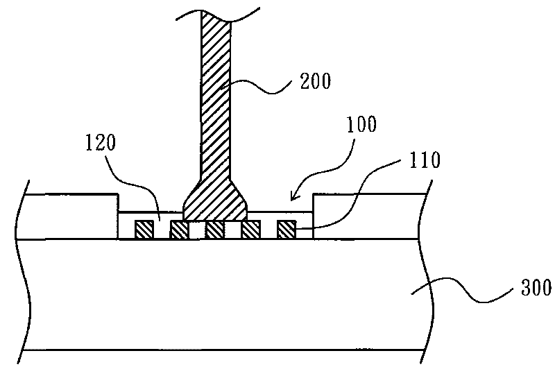
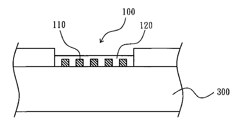
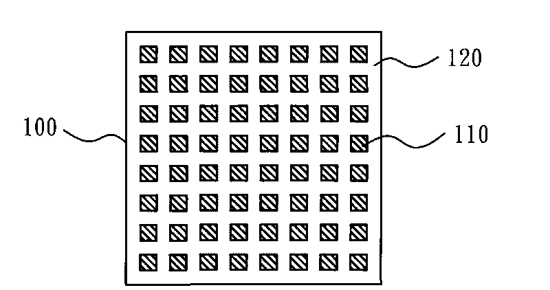
[0028] Please refer to figure 1 , which shows a schematic cross-sectional view of a wire bonding structure according to an embodiment of the present invention. The pad structure 100 of this embodiment is used to bond (eg solder) the wire 200 to form a wire bonding structure, which can be applied in a packaging structure for electrical connection. The pad structure 100 includes a patterned structure 110. The patterned structure 110 has a first material whose hardness is greater than that of the wire 200, and the distribution area of ​​the patterned structure 110 in the pad structure 100 is larger than that of the wire 200 and the wire. The contact area between the pad structures 100 (that is, the area of ​​the bonding surface) is used to prevent the pad from being damaged or deformed by being pressed by the wire when the hardness of the wire is greater than that of the pad.

[0029] Please refer to Figure 2 to Figure 3E , figure 2 A schematic cross-sectional view showing ...


PUM


Abstract

The invention provides a pad connecting structure, a lead wire jointing structure and an encapsulating structure. The lead wire jointing structure comprises the pad connecting structure and a lead wire, the pad connecting structure comprises a pattern structure and a second material, the pattern structure is provided with a first material, the lead wire is jointed with the pad connecting structure, the material rigidity of the lead wire is lower than that of the first material, and the distribution area of the pattern structure is larger than the contact area between the lead wire and the padconnecting structure. The pad connecting structure and the lead wire jointing structure can be applied in the encapsulating structure, so as to ensure the routing quality and to reduce the stripping problems between the lead wire and a connecting pad.

Description

technical field [0001] The invention relates to a pad structure, a wire bonding structure and a packaging structure, in particular to a pad structure, a wire bonding structure and a packaging structure capable of ensuring the quality of bonding. Background technique [0002] In the manufacturing process of semiconductor packaging, wire bonding technology has been widely used in the electrical connection between semiconductor chips and packaging substrates or lead frames. Generally, the wire bonding process is mainly based on gold wires, but because copper wires have the advantage of low cost, compared with gold wires, copper wires have better electrical and thermal conductivity, so the wire diameter of copper wires can be smaller than that of gold wires. Thin and better heat dissipation efficiency. [0003] see Figure 7 , which shows a schematic cross-section according to an existing wire bonding. At present, the copper bonding wire 910 can be bonded to the pad 920 by a w...

Claims


Application Information

Patent Timeline
IPC IPC(8): H01L23/488H01L23/49H01L23/498H01L23/485H01L23/31
CPCH01L2224/05559H01L2924/01046H01L24/03H01L2224/78301H01L2924/01082H01L2924/01047H01L24/05H01L2924/01079H01L24/78H01L24/85H01L2224/48227H01L2924/01033H01L2924/01029H01L2924/01028H01L2224/48091H01L2924/01013H01L2224/48464H01L2224/45147H01L2224/85181H01L2224/02166H01L2224/04042H01L2224/45015H01L2224/48H01L2224/48463H01L2224/78H01L2224/85H01L2224/85205H01L2924/00011H01L2924/181H01L2924/00014H01L2924/00H01L2924/207H01L2924/00012H01L2924/01005
Inventor 许宏达
Owner ASE ASSEMBLY & TEST SHANGHAI
Learn More