


Quick Research
Generate reliable direction feasibility study reports for your R&D in just a few steps.

Technical Q&A
Discover and master advanced knowledge NOW. Basics, ideas, possibilities, all at once.

Find Solutions
As an expert in R&D theories, this can generate solutions to your technical problems instantly.

Evaluate Feasibility
Analyze your overall solution with one click, know your potential R&D risks in advance.

Monitor Landscape
Get weekly tech updates, stay abreast of the latest tech innovations and key insights.
Optical element and production method of the same
A manufacturing method and technology of an optical device, which are used in the manufacture of optical elements, optical heads, recording/reproducing by optical methods, etc., to achieve the effects of suppressing light absorption, improving light transmittance, suppressing aberration variation and reducing transmittance. Effect
- Summary
- Abstract
- Description
- Claims
- Application Information
AI Technical Summary
Problems solved by technology
Method used
Image

Examples
Embodiment 1
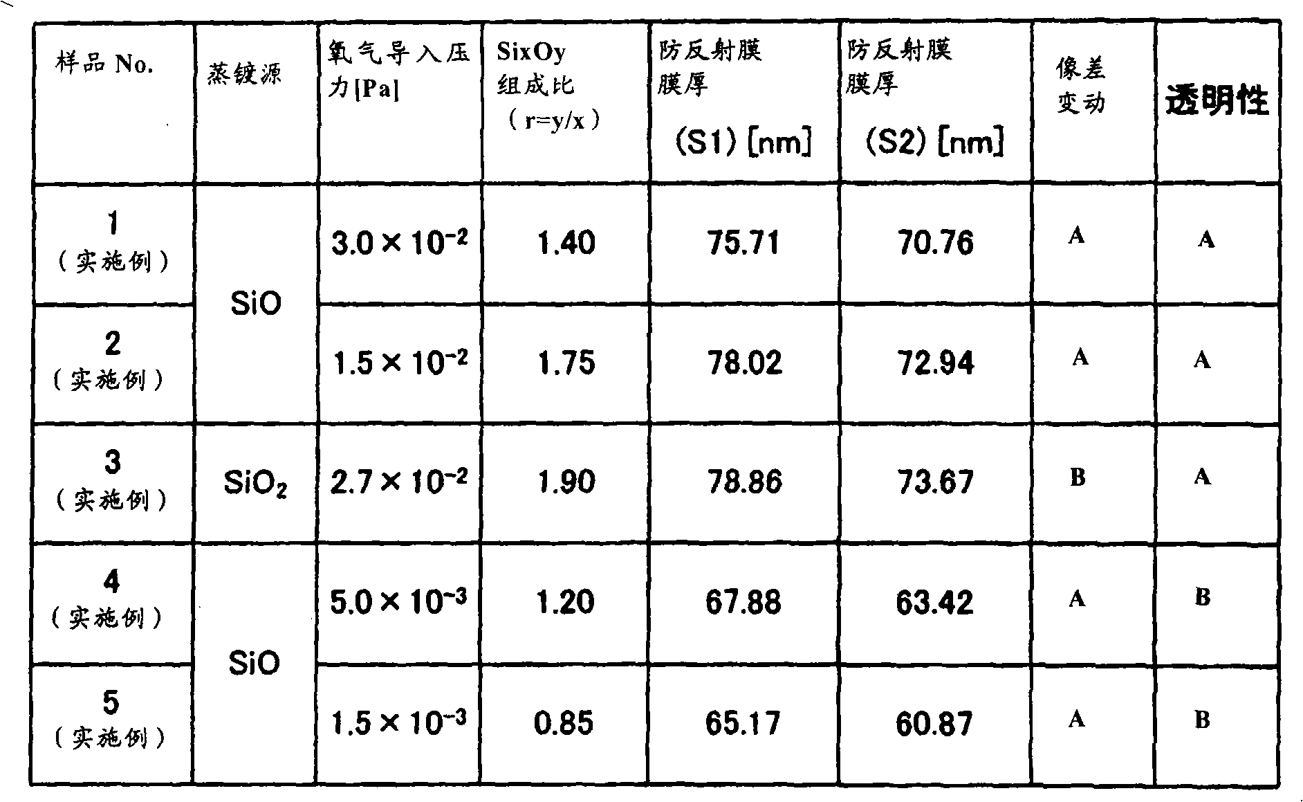
[0066] (1) Manufacturing of samples
[0067] On the incident side and the emitting side surface of a resin lens base material (objective lens for blue light) manufactured using a cyclic olefin resin (APEL manufactured by Mitsui Chemicals), the thickness described in Table 2 is formed as follows. x o y Anti-reflective film composed of a single layer.
[0068] The anti-reflection film of each sample was formed by the vacuum evaporation method. When forming each of these films, while appropriately changing the introduction pressure of the evaporation source and oxygen, five types of samples were formed. According to the conditions, "Sample No. 1" was formed. ~5". Table 2 shows the vapor deposition conditions of samples No. 1 to 5. Table 2 shows the film thickness of the antireflection film, and the composition ratio r(Si x o y y / x values in ).
[0069] In addition, the composition ratio r in Table 2 is a value calculated from the amount of element present obtained by X-ra...
Embodiment 2
[0081] (1) Manufacturing of samples
[0082]On the surface of the incident side and the emitting side of the resin lens substrate (objective lens for blue light) manufactured by using the cyclic olefin resin (Mitsui Chemicals APEL) manufactured in the same manner as in Example 1, the film thicknesses shown in the following Table 3 were used to form antireflection. membrane. In Table 3, the layer closest to the substrate side is regarded as the lower layer, and the layer farthest from the substrate side is regarded as the upper layer, and the same composition ratio r(Si x o y y / x value in ) silicon oxide film. As the intermediate layer, a zirconia layer having a refractive index of 1.93 for light of 400 nm was used. As the design wavelength (the wavelength at which the reflectance becomes the lowest), consider the shape of the lens surface and the total transmittance, and set it as 470nm on the incident surface side (S1 surface side) and 440nm on the exit surface side (S2 su...
PUM
| Property | Measurement | Unit |
|---|---|---|
| refractive index | aaaaa | aaaaa |
| refractive index | aaaaa | aaaaa |
| refractive index | aaaaa | aaaaa |
Abstract
Description
Claims
Application Information
 - R&D Engineer
- R&D Manager
- IP Professional
- Industry Leading Data Capabilities
- Powerful AI technology
- Patent DNA Extraction
Browse by: Latest US Patents, China's latest patents, Technical Efficacy Thesaurus, Application Domain, Technology Topic, Popular Technical Reports.
© 2024 PatSnap. All rights reserved.Legal|Privacy policy|Modern Slavery Act Transparency Statement|Sitemap|About US| Contact US: help@patsnap.com