
Two-dimensional vertical-cavity surface-emitting laser array with high light beam quality

A vertical cavity surface emission, high-beam technology, applied in lasers, laser components, semiconductor lasers, etc., can solve problems such as complex structures, increased overall device volume, and limited laser power density, to achieve expanded application fields and reliability High, improve the effect of output beam quality

Inactive Publication Date: 2010-02-03
CHANGCHUN INST OF OPTICS FINE MECHANICS & PHYSICS CHINESE ACAD OF SCI
View PDF0 Cites 11 Cited by
  • Summary
  • Abstract
  • Description
  • Claims
  • Application Information

AI Technical Summary

Problems solved by technology

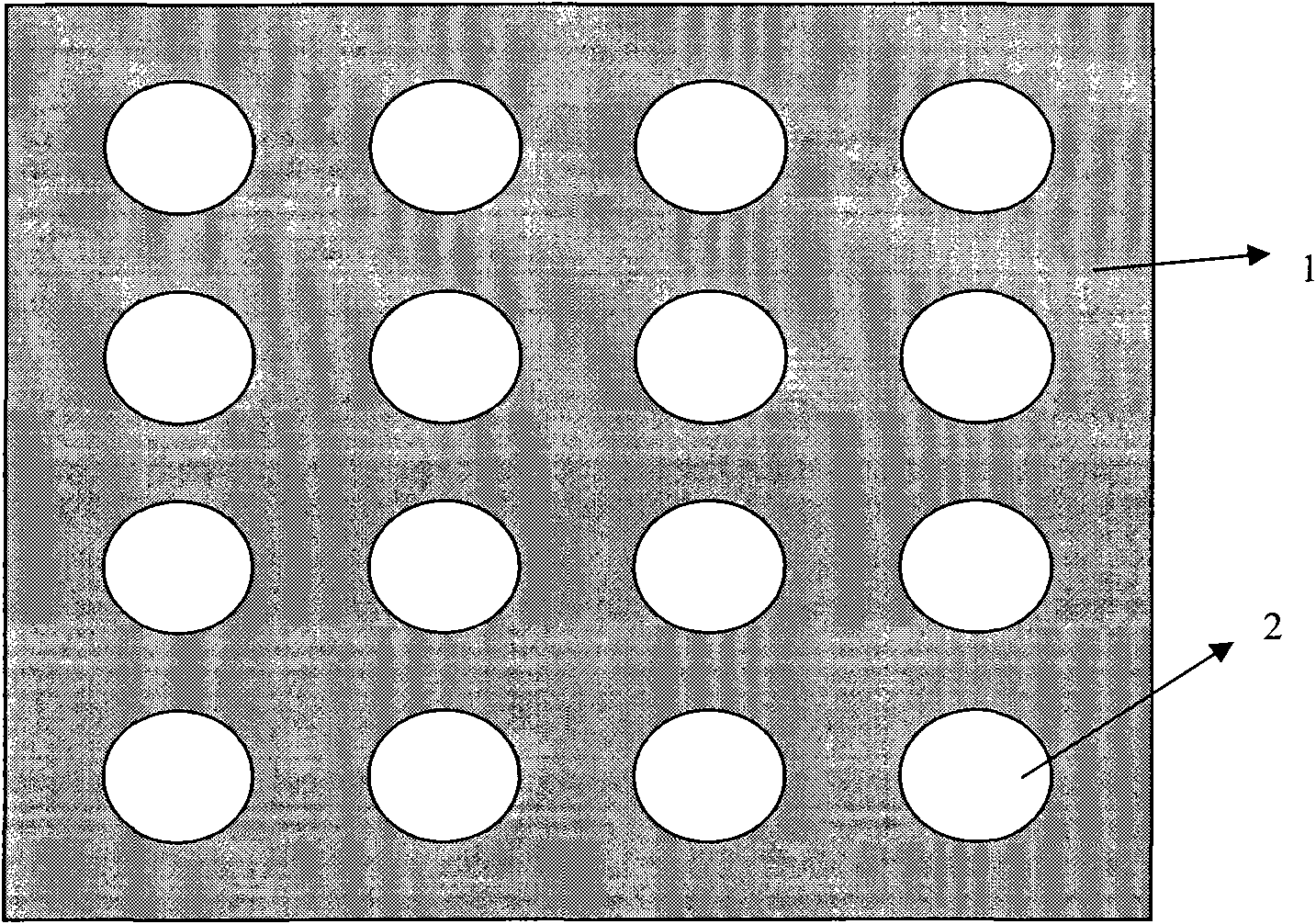
[0003] The main defect of this laser array is that the ring-shaped or circular beams of each unit laser device 2 are superimposed to form a periodic intensity distribution with a series of peaks in the far field. This kind of laser far field limits the increase of laser power density , requires a complex optical system for processing, which increases the overall volume of the device and complicates the structure

Method used


Image

  • Two-dimensional vertical-cavity surface-emitting laser array with high light beam quality
  • Two-dimensional vertical-cavity surface-emitting laser array with high light beam quality

Examples


Embodiment Construction

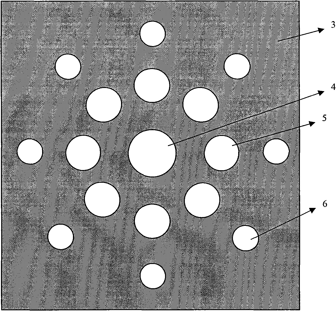
[0011] The invention according to figure 2 The structure shown is implemented, wherein the surface electrode 3 is made by evaporation, the diameter of the light exit hole of the single unit laser device 4 in the central area is 200 μm, and the power is 530 mW, and the diameter of the light exit hole of the first ring unit laser device 5 is 150 μm. The diameter of the light exit hole of the second ring unit laser device 6 is 100 μm, and the power is 100 mW. The distance between the first ring and the single unit laser device 4 in the central area is 300 μm, and the distance between the second ring and the first ring is 250 μm. Firstly, a set of photolithography masks required is fabricated according to the structure, and then the traditional oxidation-limited vertical cavity surface emitting laser process flow is used to fabricate the two-dimensional vertical cavity surface emitting laser array with high beam quality. The unit laser devices in this technical solution all use ...


PUM


Abstract

The invention discloses a two-dimensional vertical-cavity surface-emitting laser array with high light beam quality, belonging to the technical filed of a semiconductor laser device, and relating to alaser device array. The invention aims to solve the technical problems of providing a two-dimensional vertical-cavity surface-emitting laser array with high light beam quality. The technical scheme to solve the technical problems comprises a surface electrode, a central zone single unit laser device, first circular ring unit laser devices and second circular ring unit laser devices, wherein, thecenter of the array is the central zone single unit laser device, and the first circular ring unit laser devices are evenly distributed on a concentric circular ring on the outer side of the array; the second circular ring unit laser devices are evenly distributed on the concentric circular ring on the outer side of the first circular ring, and the number of the first and the second circular ringunit laser devices is same; the diameters of the unit laser devices on the same circular ring are same, and the diameters of the unit laser devices on different circular rings respectively reduce frominternal to external; the central zone unit laser device and the unit laser devices on the same direction of each concentric circular ring are in rayed arrangement on the same radius.

Description

Technical field: [0001] The invention belongs to the technical field of semiconductor laser devices, and relates to a two-dimensional vertical cavity surface emitting semiconductor laser array. Background technique: [0002] Vertical cavity surface emitting laser is a new type of semiconductor laser, which has important applications in optical communication and other fields. In recent years, the needs of laser medical treatment, laser pumping and laser storage have put forward higher requirements for the power output of vertical cavity surface emitting lasers. In order to obtain high power output, the light exit aperture of a single-tube vertical cavity surface emitting laser generally needs to be hundreds of microns. The large aperture light exit window causes uneven current density at each point in the light exit hole, especially near the edge of the oxidation-limited region. , there is a strong current aggregation effect, resulting in uneven light emission in the light e...

Claims


Application Information

Patent Timeline
Patent Type & Authority Applications(China)
IPC IPC(8): H01S5/42
Inventor 李特宁永强刘云秦莉王立军张岩张立森
Owner CHANGCHUN INST OF OPTICS FINE MECHANICS & PHYSICS CHINESE ACAD OF SCI
Learn More