
Low-loss surface plasmon optical waveguide structure

A surface plasmon, low-loss technology, applied in the direction of optical waveguide and light guide, can solve the problem of large waveguide transmission loss, etc., and achieve the effects of good confinement, low effective refractive index, and flat dispersion characteristics

Inactive Publication Date: 2010-01-20
THE NAT CENT FOR NANOSCI & TECH NCNST OF CHINA +1
View PDF0 Cites 20 Cited by
  • Summary
  • Abstract
  • Description
  • Claims
  • Application Information

AI Technical Summary

Problems solved by technology

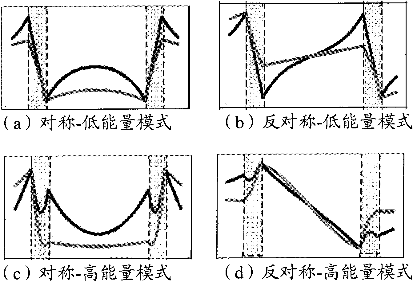
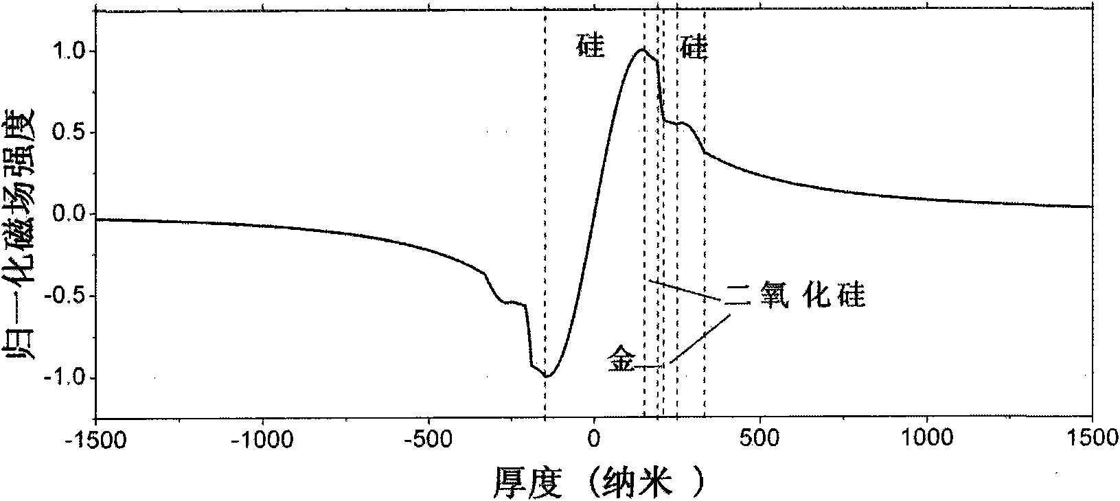
[0013] The purpose of the present invention is to overcome the defect of large transmission loss of traditional metal / dielectric / metal surface plasmon optical waveguides, thereby providing a surface plasmon optical waveguide structure capable of transmitting antisymmetric-high energy modes with low loss

Method used


Image

  • Low-loss surface plasmon optical waveguide structure
  • Low-loss surface plasmon optical waveguide structure
  • Low-loss surface plasmon optical waveguide structure

Examples


Embodiment Construction

[0030] Two important indicators of surface plasmon waveguides are their field confinement ability and transmission loss. The field confinement capability can be determined by the effective mode field area A eff To represent, the expression is as follows:

[0031] A eff =(∫∫|E(x,y)| 2 dxdy) 2 / ∫∫|E(x,y)| 4 dxdy (1)

[0032] where A eff is the effective mode field area, and E(x, y) is the electric field of the surface plasmon wave.

[0033] The expression of transmission loss Loss is as follows:

[0034] Loss=20log(e)k 0 Im(N eff )≈8.686k 0 Im(N eff )(dB / m) (2)

[0035] where Im(N eff ) is the imaginary part of the effective refractive index of the mode, k 0 Indicates the wavenumber of light in vacuum. The size of the transmission loss determines the transmission distance of light in the medium. Transmission distance L p It is defined as the distance when the electric field intensity on any interface decays to the initial value l / e, and the relational expression...


PUM


Abstract

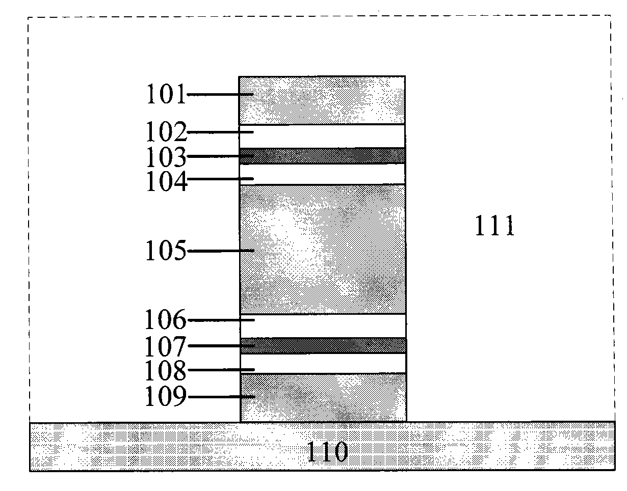
The invention relates to the technical fields of surface plasmon optical waveguide structures and provides an antisymmetric-high energy mode surface plasmon optical waveguide structure capable of low-loss transmission for overcoming a large loss drawback of the conventional metal / media / metal waveguide transmission. The optical waveguide structure realizes a waveguide structure for supporting transmission in an antisymmetric-high energy mode by combining the refractive index difference between a plurality of high refractive index layers and a low refractive index substrate and a low refractive index covering layer and a surface plasmon effect of a metal layer and uses the low refractive index medium layers on two sides of the metal layer to reduce transmission loss, thereby realizing low-loss surface plasmon optical waveguide. Meanwhile, the optical waveguide structure has the advantages of small effective mode filed area and low loss can be used for manufacturing optical devices of a subwavelength size and ultra high integration level optical circuits.

Description

technical field [0001] The invention relates to the field of optical waveguide structures, in particular to surface plasmon optical waveguide structures with low loss. Background technique [0002] A surface plasmon is a pattern of electromagnetic waves caused by the interaction of light and free electrons on the surface of a metal. This mode exists near the metal-dielectric interface, and its field strength reaches its maximum at the interface, and decays exponentially on both sides of the interface along the direction perpendicular to the interface. Surface plasmons have strong field confinement properties, which can confine the field energy to a region whose spatial size is much smaller than its free-space wavelength, and its properties can change with the change of the metal surface structure. In a waveguide structure composed of appropriate metals and dielectrics, surface plasmons can be confined to a range of tens of nanometers or even smaller, and are no longer affec...

Claims


Application Information

Patent Timeline
Patent Type & Authority Applications(China)
IPC IPC(8): G02B6/10
Inventor 郑铮赵欣卞宇生朱劲松范江峰
Owner THE NAT CENT FOR NANOSCI & TECH NCNST OF CHINA
Learn More