Cosine signal and Chirp signal combined signal modulating and demodulating method, and signal transmitting and receiving method based on the method
A chip signal and signal modulation technology, applied in the direction of phase modulation carrier system, etc., can solve the problems of non-orthogonal performance and low system capacity, so as to improve the utilization rate, improve the system capacity, and reduce the transmission bit error rate. worsening effect
- Summary
- Abstract
- Description
- Claims
- Application Information
AI Technical Summary
Problems solved by technology
Method used
Image
Examples
specific Embodiment approach 1
[0028] Embodiment 1: A signal modulation and demodulation method combining cosine and chip signals, characterized in that: Modulation method: 4 binary digital signals obtained after serial / parallel conversion and 4 orthogonal intermediate frequency signals Modulation to obtain 4 channels of modulation signals; demodulation method: match and correlate the mixed signal to be demodulated with 4 channels of orthogonal intermediate frequency signals, and then perform integral judgment demodulation to obtain demodulation information;
[0029] The four-way orthogonal intermediate frequency signals are two-way QPSK carrier signals cos(2πf c t), sin(2πf c t) and two chip signals cos(2πf c t+kπt 2 ), sin(2πf c t+kπt 2 ), where f c is the center frequency of the QPSK carrier signal, k is the sweep speed, and the four signals are orthogonal or quasi-orthogonal to each other.
[0030] The sweep speed k is given by the formula:
[0031] k=B / (T / 2)=4 / T 2
[0032] Definitely, where T ...
specific Embodiment approach 2
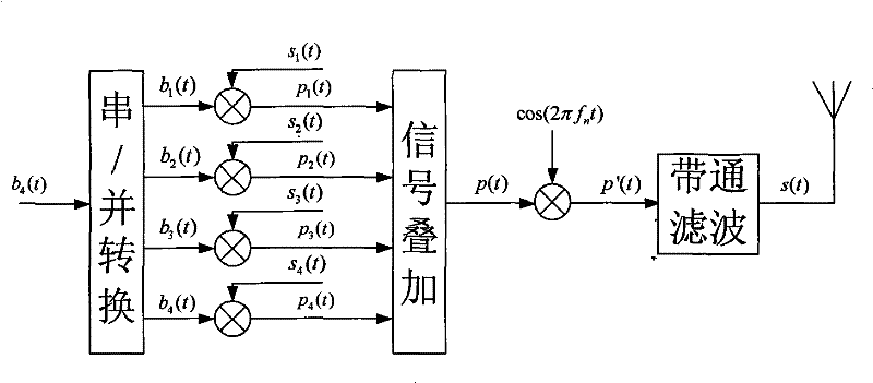
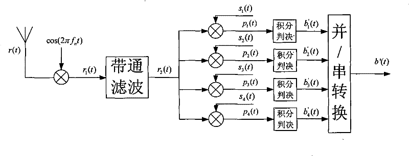
[0072] Specific implementation mode two: combination figure 1 and figure 2 This specific embodiment will be described. Described in this specific embodiment is based on the signal transmission and reception method of the signal modulation and demodulation method of a kind of cosine and Chip signal combination described in specific embodiment one, and its steps are:
[0073] Launch process:
[0074] Step 1: Perform serial / parallel conversion of the binary digital signal b(t) to be sent with a code rate of 4Rbit / s to obtain four signals b n (t), the code rate of each signal is reduced to Rbit / s, and R takes a positive integer;
[0075] Step 2: The four-way signal b obtained in step 1 n (t) and four quadrature intermediate frequency signals s n (t) Modulate to obtain four modulation signals p n (t)=b n (t)·s n (t);
[0076] Step 3: The four modulation signals p obtained in Step 2 n (t) superposition, to obtain the superimposed signal p(t);
[0077] Step 4: Perform up-...
PUM
 Abstract
Description
Claims
Application Information
 - Generate Ideas
- Intellectual Property
- Life Sciences
- Materials
- Tech Scout
- Unparalleled Data Quality
- Higher Quality Content
- 60% Fewer Hallucinations
Browse by: Latest US Patents, China's latest patents, Technical Efficacy Thesaurus, Application Domain, Technology Topic, Popular Technical Reports.
© 2025 PatSnap. All rights reserved.Legal|Privacy policy|Modern Slavery Act Transparency Statement|Sitemap|About US| Contact US: help@patsnap.com


