File conversion system and file conversion method

A file transfer and file setting technology, applied in the field of semiconductor testing, can solve the problems of delayed product delivery time, complicated transfer steps, and difficult handover, etc., so as to reduce the preparation time for mass production, reduce the probability of claims, and reduce human negligence. Effect

Active Publication Date: 2011-07-06
KING YUAN ELECTRONICS
View PDF1 Cites 0 Cited by
  • Summary
  • Abstract
  • Description
  • Claims
  • Application Information

AI Technical Summary

Problems solved by technology

Such a file conversion program is quite time-consuming. For example, based on the calculation of testing 10 products (including different software codes of the same product) every day, it takes about three or four hours a day for file conversion; Due to the requirement of file transfer, the engineer in charge must work overtime to meet customer needs
In addition, it often happens that when receiving the goods to be tested from the customer, there is no test mode to test because the staff is absent and cannot transfer files; Unable to obtain the test mode, resulting in delays in product delivery, or even testing in the wrong test mode and causing customer claims
In addition to the long conversion time, too many conversion steps, difficult handover, and error-prone, other disadvantages of the above-mentioned conversion procedures include the variety of types that must be converted, human error prone to occur, and the lead time for mass production is too long, etc. and other defects
[0007] It can be seen that the above-mentioned existing shifting system and shifting method thereof obviously still have inconvenience and defects in shifting method, product structure and use, and need to be further improved urgently
In order to solve the above-mentioned problems, the relevant manufacturers have tried their best to find a solution, but no suitable design has been developed for a long time, and there is no suitable method and structure for general methods and products to solve the above-mentioned problems. This is obviously a problem that relevant industry players are eager to solve

Method used


Image

  • File conversion system and file conversion method
  • File conversion system and file conversion method
  • File conversion system and file conversion method

Examples


Embodiment Construction

[0040] In order to further explain the technical means and effects of the present invention to achieve the intended purpose of the invention, the specific implementation methods, methods, Steps, structures, features and effects thereof are described in detail below.

[0041] The aforementioned and other technical contents, features and effects of the present invention will be clearly presented in the following detailed description of preferred embodiments with reference to the drawings. Through the description of the specific implementation mode, when the technical means and functions adopted by the present invention to achieve the predetermined purpose can be obtained a deeper and more specific understanding, but the accompanying drawings are only for reference and description, and are not used to explain the present invention be restricted.

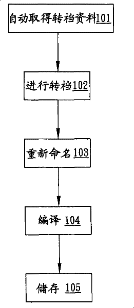
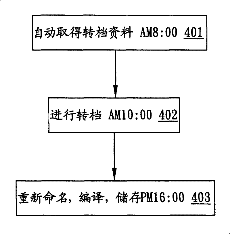
[0042] see figure 1 Shown is a flow chart of the shifting method in a preferred embodiment of the present invention. The main purpo...


PUM


Abstract

The invention relates to a file conversion system and a file conversion method. The file conversion method comprises the following steps: automatically obtaining file conversion data containing a testmode to be converted; carrying out file conversion so as to convert the test mode to be converted into a format of a target test mode; renaming the target test mode after the file conversion; compiling the target test mode; and storing the renamed target test mode. The file change system comprises a file conversion server and at least one test machine for testing a wafer, wherein the file conversion server is used for automatically obtaining the file conversion data containing the test mode to be converted, converting the test mode to into the target test mode, renaming the target test mode,compiling the target test mode and storing the renamed target test mode. The invention ensures that file conversion steps can be simplified, unified and automatically operated completely. A test module after the file conversion can be repeatedly used so as to reduce man-made careless mistakes and staff for extra hour work, improve the working efficiency, reduce mass-production preparation time, have high system extendibility and reduce the relevant cost.

Description

technical field [0001] The present invention relates to a shifting system and a shifting method thereof, in particular to a simplified and unified shifting step, which can be fully automated, and the target test module after shifting can be reused, reducing human error and improving work The conversion system and the conversion method in the semiconductor testing field have high efficiency and high system scalability and can reduce related costs. Background technique [0002] In the field of semiconductor testing, a testing system such as a probe card system is usually used, and its precise contact mechanism is in contact with the wafer to be tested to form an electrical path and perform the test. Wherein, the semiconductor test system transmits the test pattern to a test interface, and then transfers it to the probe card and successively contacts the chips to be tested on the wafer, and then transmits the test pattern back through the same path. This test interface can als...

Claims


Application Information

Patent Timeline
Patent Type & Authority Patents(China)
IPC IPC(8): G06F17/27
Inventor 郑世杰刘龙昌
Owner KING YUAN ELECTRONICS
Why Eureka
Try Eureka