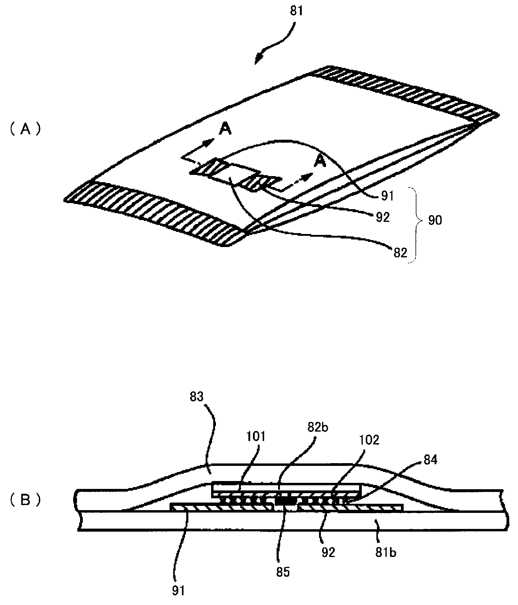
Radio IC device and component for radio IC device
A device, wireless technology, applied in the direction of electric solid devices, semiconductor devices, antenna components, etc., can solve the problems of inability to install IC marks, thickening of the IC mark forming part, and increase in the manufacturing cost of the packaging body.
- Summary
- Abstract
- Description
- Claims
- Application Information
AI Technical Summary
Problems solved by technology
Method used
Image
Examples
no. 1 Embodiment approach 》
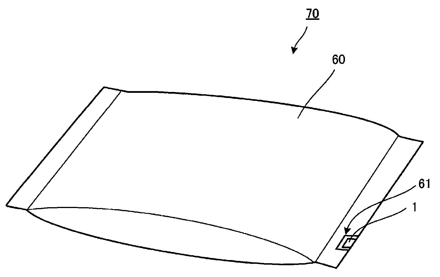
[0153] figure 2 It is a perspective view of the external appearance of the wireless IC device of the first embodiment and an article including the device. The article 70 is, for example, bagged snacks such as bagged potato chips, and the article package 60 is a bag-shaped package made of an aluminum vapor-deposited laminated film.
[0154] A notch (a portion where aluminum vapor deposition is not performed) 61 is formed at the edge of the article package 60 , and the electromagnetic coupling module 1 is placed in the notch 61 .
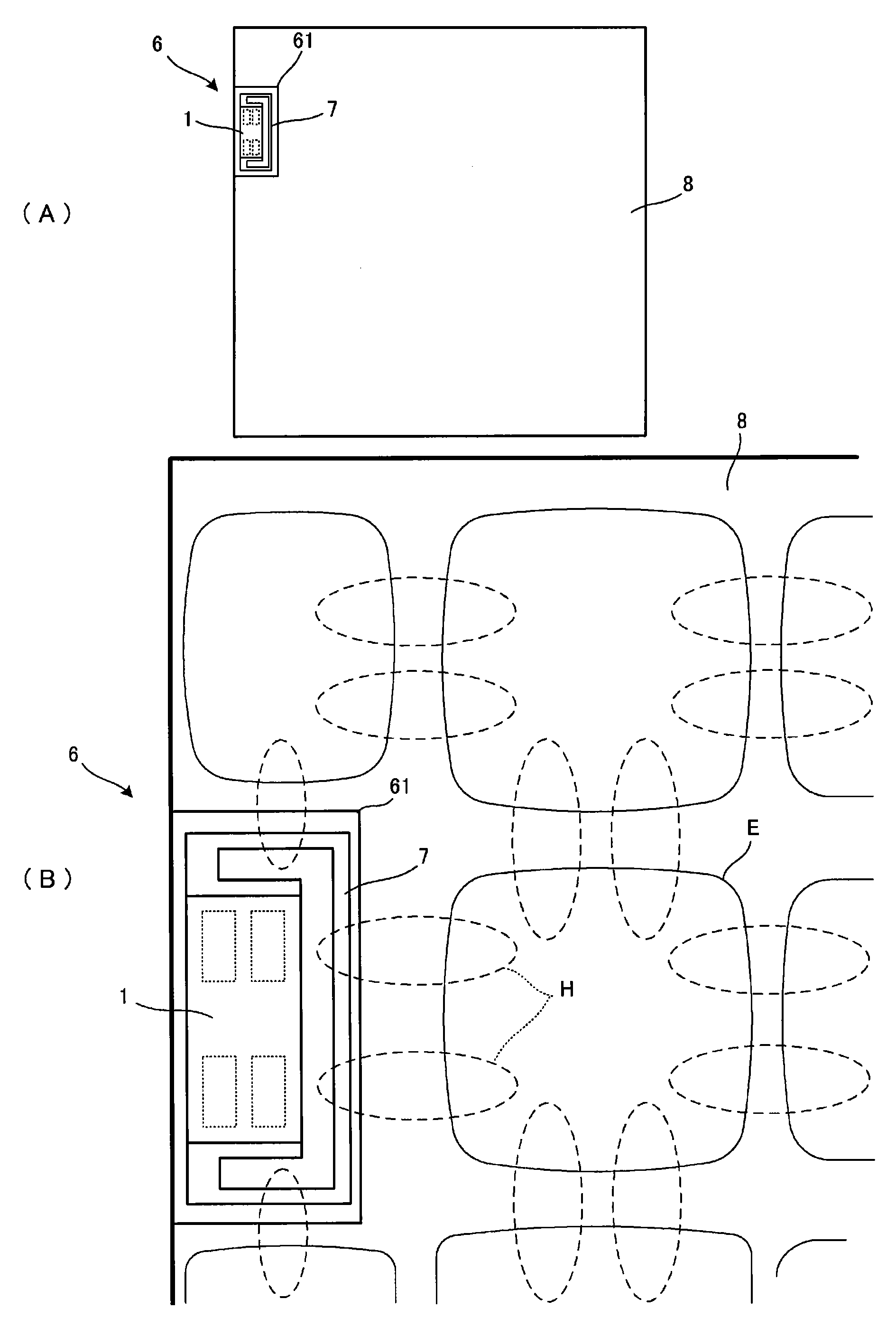
[0155] image 3 is a block diagram representing a wireless IC device, showing only figure 2 Elemental portions of article 70 are shown. image 3 , the radiation electrode 8 with figure 2 The aluminum vapor-deposition layer of the aluminum vapor-deposition laminated film of the illustrated article packaging body 60 is equivalent. A ring-shaped electrode 7 is formed inside the notch portion (electrode non-formation portion) 61 of the radiation e...
no. 2 Embodiment approach 》
[0163] Figure 4 It is a perspective view of the external appearance of the wireless IC device and the article including the device according to the second embodiment. The article 71 is, for example, a packaged confectionery, and the article package 60 is a bag-shaped package formed of an aluminum vapor-deposited laminated film.
[0164] figure 2 In the example shown, the electromagnetic coupling module is arranged on the edge of the article package, but the Figure 4 In the example shown, the electromagnetic coupling module 1 is provided inside the edge part away from the article packaging body 60 . The article packaging body 60 is formed of an aluminum vapor-deposited laminated film, and a non-conductive portion 62 is formed in a part of the aluminum-deposited laminated film, and the electromagnetic coupling module 1 is disposed inside and at an end of the non-conductive portion 62 .
[0165] Figure 5 yes means Figure 4 The structural diagram of the installation part...
no. 3 Embodiment approach 》
[0169] Image 6 (B) is a configuration diagram showing main parts of the wireless IC device of the third embodiment, Image 6 (A) is an external view of an article including the wireless IC device. Image 6 In (A), the article 72 has the main part 6 of the wireless IC device on the metal plane body 63 . The flat metal body 63 is a plate-shaped or sheet-shaped article containing a metal layer inside or the metal plate itself.
[0170] The main parts of wireless IC devices6 such as Image 6 As shown in (B), the overall shape is in the shape of a so-called index strip (Japanese タッツズインデェンデズス), and an adhesive layer is provided on the inner surface of the insulating sheet 64, and the ring-shaped electrode 7 and the electromagnetic coupling module 1 are sandwiched by the insulating sheet 64. into it. The structure and structure of the ring electrode 7 and the electromagnetic coupling module 1 image 3 The situation shown is the same.
[0171] Then, install the ring electrode 7...
PUM
 Abstract
Description
Claims
Application Information
 - Generate Ideas
- Intellectual Property
- Life Sciences
- Materials
- Tech Scout
- Unparalleled Data Quality
- Higher Quality Content
- 60% Fewer Hallucinations
Browse by: Latest US Patents, China's latest patents, Technical Efficacy Thesaurus, Application Domain, Technology Topic, Popular Technical Reports.
© 2025 PatSnap. All rights reserved.Legal|Privacy policy|Modern Slavery Act Transparency Statement|Sitemap|About US| Contact US: help@patsnap.com


