
Mid-frequency direct current compound magnetron sputtering device

A magnetron sputtering device and magnetron sputtering technology, applied in the direction of sputtering coating, ion implantation coating, metal material coating process, etc., can solve the problems of high investment cost, inconvenient use, and flexibility, etc., and achieve Uniform coating effect

Inactive Publication Date: 2009-09-23
HUZHOU JINTAI PLATING IND
View PDF0 Cites 7 Cited by
  • Summary
  • Abstract
  • Description
  • Claims
  • Application Information

AI Technical Summary

Problems solved by technology

However, the existing magnetron sputtering equipment that can accurately control and plate large-area compound thin films and multilayer films has high investment costs and is not convenient and flexible enough to use.

Method used

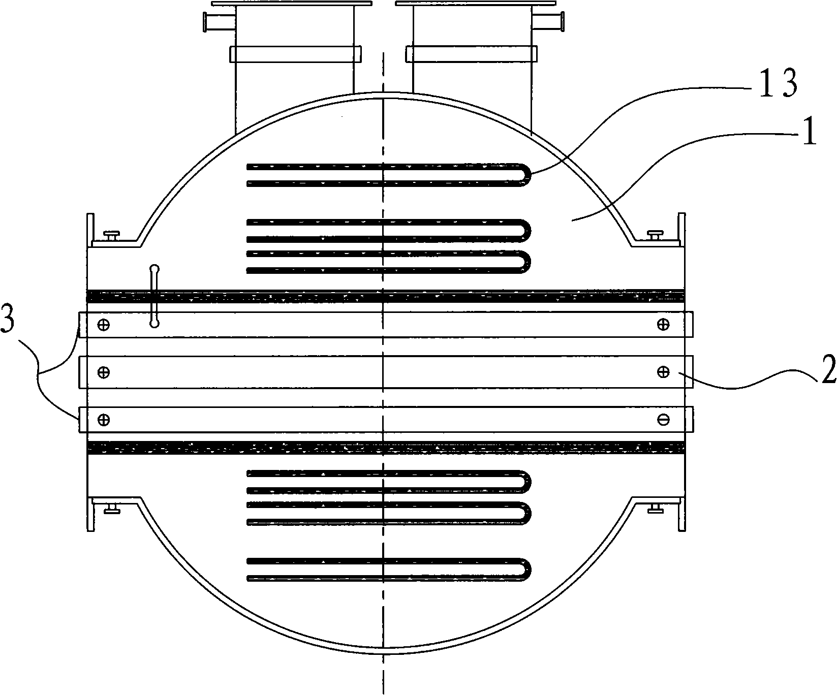
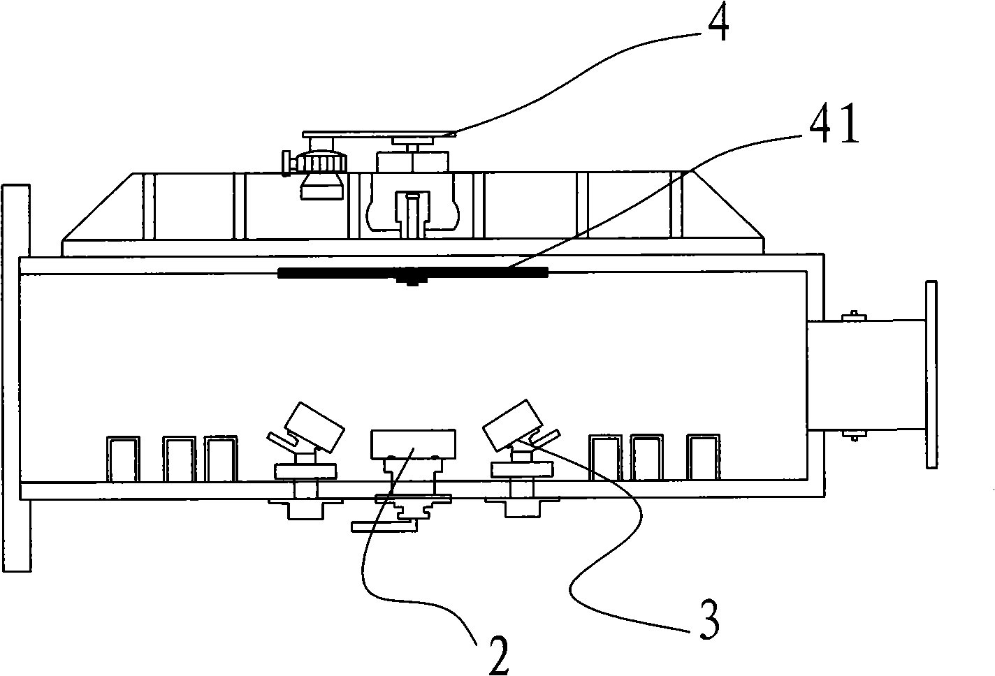
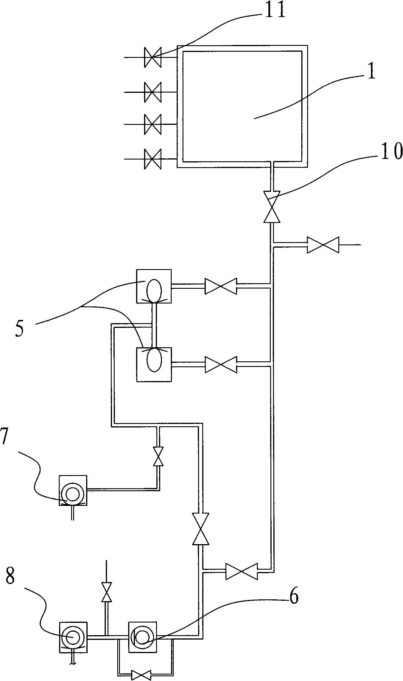

Image

  • Mid-frequency direct current compound magnetron sputtering device
  • Mid-frequency direct current compound magnetron sputtering device
  • Mid-frequency direct current compound magnetron sputtering device

Examples


Embodiment Construction

[0026] The present invention will be described in further detail below in conjunction with the accompanying drawings.

[0027] This specific embodiment is only an explanation of the present invention, and it is not a limitation of the present invention. Those skilled in the art can make modifications to this embodiment without creative contribution as required after reading this specification, but as long as they are within the rights of the present invention All claims are protected by patent law.

[0028] Such as figure 1 , shown in 2 and 3, a 2200-type disc-shaped horizontal intermediate frequency DC composite magnetron sputtering device, including a vacuum chamber 1, an air extraction system, an air supply system, a film thickness measurement and control system, and an electrical control cabinet (not shown), the vacuum chamber is equipped with a DC planar magnetron sputtering target 2, which is a silver target, and a pair of intermediate frequency twin magnetron sputterin...


PUM


Abstract

The invention relates to a mid-frequency direct current compound magnetron sputtering device comprising a vacuum chamber, an air extraction system, an air supply system, a film thickness measuring and controlling system and an electric control cabinet, a direct current planar magnetron sputtering target is arranged in the vacuum chamber, and a pair of mid-frequency twin magnetron sputtering targets are arranged on two sides of the direct current planar magnetron sputtering target. The device comprises the direct current planar magnetron sputtering target, and a pair of the mid-frequency twin magnetron sputtering targets are arranged on the two sides of the direct current planar magnetron sputtering target, thereby being very applicable to plating a plurality of layers of compound films and simple substance films on a substrate. The device has low manufacturing cost, convenience and flexibility.

Description

technical field [0001] The invention relates to the field of new materials and surface technology, in particular to a magnetron sputtering device for compound thin film and multilayer film materials. Background technique [0002] The two-dimensional stretched film is very important because of its special composition, structure and size effect, which enables it to obtain properties that three-dimensional materials do not have, and at the same time saves materials. For example, high-density integrated devices such as integrated circuits, integrated optical circuits, and magnetic bubbles can only be designed and manufactured by using thin films and their properties. Another example is large-area cheap solar cells and many important optoelectronic devices. Only by using expensive semiconductor materials and other precious materials in the form of thin films can they be full of vitality. [0003] There are many methods for preparing thin films, and there are many types of corres...

Claims


Application Information

Patent Timeline
IPC IPC(8): C23C14/35
Inventor 钱苗根宋兴文
Owner HUZHOU JINTAI PLATING IND
Learn More