Electro-optical device and method of manufacturing electro-optical device

An electro-optical device and manufacturing method technology, applied in semiconductor/solid-state device manufacturing, circuits, optics, etc., capable of solving problems such as inability to fully reduce display quality, degradation, and inability to adequately block

Inactive Publication Date: 2009-09-02
SEIKO EPSON CORP
View PDF2 Cites 0 Cited by
  • Summary
  • Abstract
  • Description
  • Claims
  • Application Information

AI Technical Summary

Problems solved by technology

[0005] However, in the above-mentioned liquid crystal device, since the light-shielding film is flat, light incident on the TFT from a lateral direction or an oblique direction cannot be sufficiently blocked, and there is a problem that a decrease in display quality due to leakage current cannot be sufficiently reduced.

Method used


Image

  • Electro-optical device and method of manufacturing electro-optical device
  • Electro-optical device and method of manufacturing electro-optical device
  • Electro-optical device and method of manufacturing electro-optical device

Examples


Embodiment Construction

[0034] Hereinafter, as an example of an electro-optical device, a transmissive liquid crystal device of an active matrix driving type with a built-in drive circuit is taken as an example of the embodiments of the present invention, and reference is made to Figure 1 to Figure 6 Be explained. In addition, in each of the drawings shown below, the dimensions and ratios of the respective constituent elements are suitably different from the actual ones in order to make the respective constituent elements recognizable on the drawings.

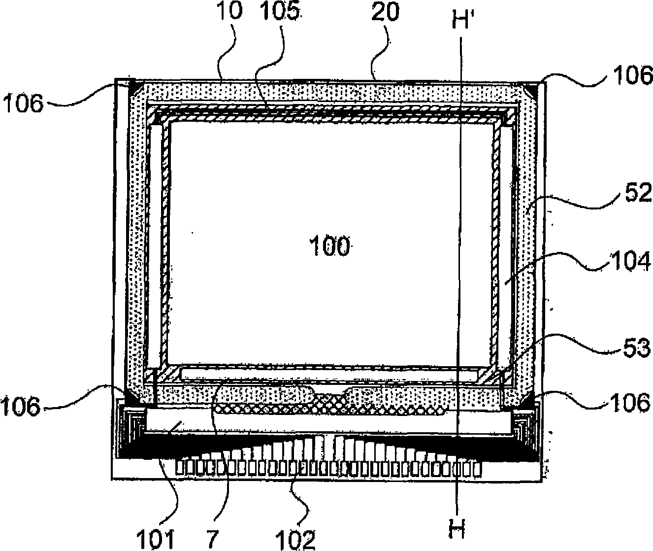
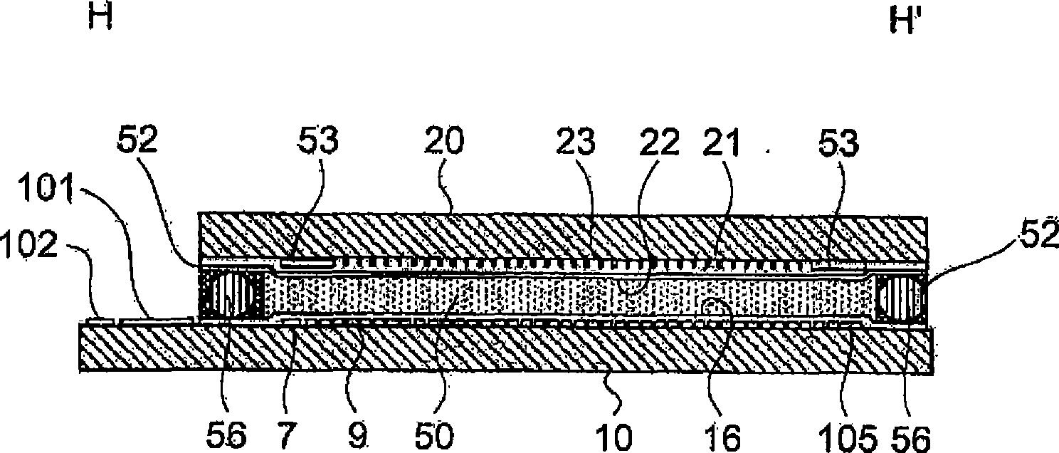
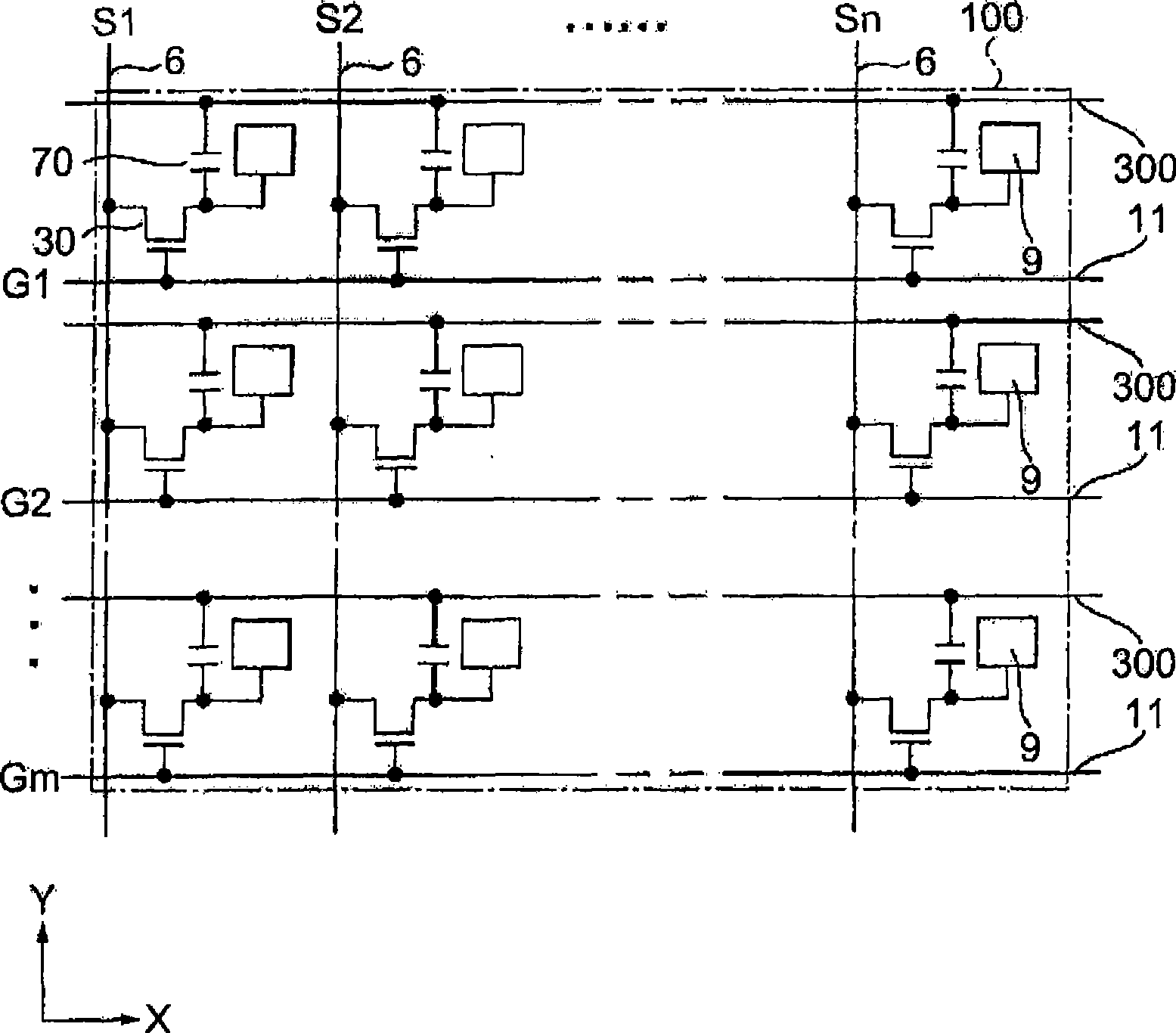
[0035] First, regarding the overall structure of the liquid crystal device in this embodiment mode, refer to figure 1 and figure 2 Be explained. figure 1 It is a schematic plan view of the element substrate 10 and components formed thereon viewed from the counter substrate 20 side of the liquid crystal device, figure 2 ,yes figure 1 A rough cross-sectional view on H-H'.

[0036] exist figure 1 and figure 2 Among them, the liquid crystal devic...


PUM


Abstract

The invention relates to an electro-optical device and a manufacturing method thereof. The electro-optical device includes a substrate (10), a first light-shielding layer (73) over the substrate, a first interlayer insulating layer (41) over the first light-shielding layer (73), a transistor (30) over the first interlayer insulating layer (41), a second interlayer insulating layer (42) over the transistor (30), and a second light-shielding layer over the second interlayer insulating layer. The invention is characterized in that a semiconductor layer (10) of the transistor (30) is arranged in a way that the layer (1) is covered by the first light-shielding layer (73) from one side of the substrate (10) and that that the layer (1) is covered by the second light-shielding layer (70) from opposite side of the substrate (10); the second light-shielding layer (70) is wider than the first light-shielding layer (73); looked down, the thinnest part of the first interlayer insulating layer is between end part of the first light-shielding layer and end part of the second light-shielding layer.

Description

technical field [0001] The invention relates to an electro-optical device and a manufacturing method thereof. Background technique [0002] In recent years, electro-optical devices such as liquid crystal devices have been widely used as display units in electronic equipment such as mobile phones, portable computers, and video cameras. In such a liquid crystal device, since light reaches a liquid crystal driving TFT (Thin Film Transistor) which is a component thereof, leakage current flows, and there is a problem that the display quality may deteriorate. In order to solve such a problem, for example, Patent Document 1 discloses a liquid crystal device in which a light-shielding film is disposed on at least one of the upper layer side and the lower layer side of a TFT to suppress the incidence of light on the TFT. Furthermore, Patent Document 2 discloses a liquid crystal device in which the light reflectance of a light-shielding film is lowered on the side facing the TFT and ...

Claims


Application Information

Patent Timeline
Patent Type & Authority Applications(China)
IPC IPC(8): G02F1/1362G02F1/133H01L27/12H01L21/84
CPCG02F1/136277G02F1/136209A44C25/00A45C13/00A45C15/00A63H3/005A63H3/02A63H3/36
Inventor 茂筑宽士
Owner SEIKO EPSON CORP
Why Eureka
Try Eureka